Inorganic resistor thick film and preparing method and application of inorganic resistor thick film
A resistance and inorganic technology, applied in the direction of resistors, non-adjustable metal resistors, circuits, etc., can solve the problems of unfavorable life and health, inapplicability, lead poisoning, etc., and achieve the effects of preventing lead poisoning, increasing the use temperature, and simple operation
- Summary
- Abstract
- Description
- Claims
- Application Information
AI Technical Summary
Problems solved by technology
Method used
Image
Examples
preparation example Construction
[0032] The embodiment of the present invention further provides a method for preparing the above-mentioned inorganic resistance thick film, comprising the following steps:
[0033] Step S01, providing raw materials:
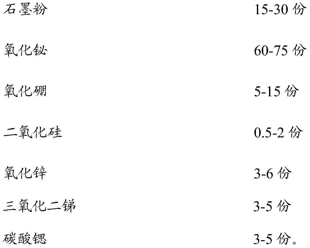
[0034] Provide the graphite powder, bismuth oxide, boron oxide, silicon dioxide, zinc oxide, antimony trioxide and strontium carbonate in proportion by weight;
[0035] Step S02, preparing the first mixture:
[0036] Heating and melting the bismuth oxide, boron oxide, silicon dioxide, zinc oxide, antimony trioxide and strontium carbonate, after cooling, grinding the melt to a mesh size below 350, adding the graphite powder and mixing to obtain a first mixture;
[0037] Step S03, preparing the second mixture:
[0038] The first mixture is mixed with the organic carrier in a weight ratio of 65-80:20-35 to obtain a second mixture;
[0039] Step S04, coating, drying and sintering:
[0040] The second mixture is coated on the substrate, dried and sintered to obtai...
Embodiment 1
[0054] Take a rectangular mica sheet with a length of 600mm, a width of 200mm, and a thickness of 0.5mm, and use it as figure 2 base plate 1 shown;
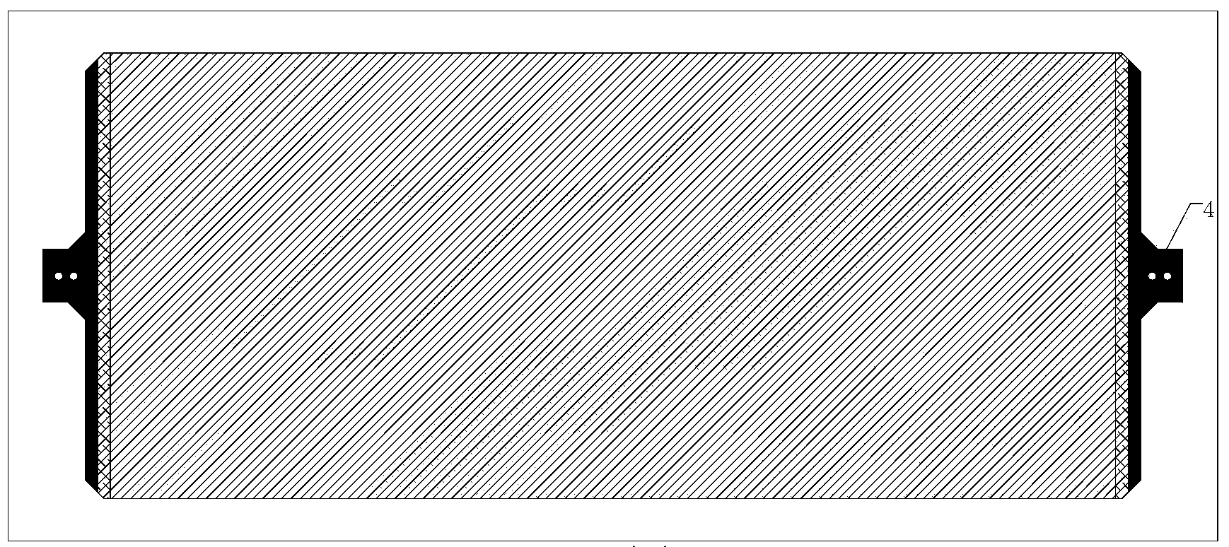
[0055] Then use silver conductive paste to coat a length of 170mm and a conductive electrode with a width of 10mm on the same side of the two short sides of the rectangular substrate, which is figure 2 The conductive electrode referred to in 3) and the lead end indicated in 4 in Figure 1, dry the bottom plate together with the conductive electrode for later use;
[0056] Provide the following formula raw materials:
[0057]
[0058]
[0059] Stir the 6 ingredients in the above formula except graphite powder evenly, melt the mixture at 1200°C for 60 minutes, cool the obtained mixture block and crush it, and then use a ball mill for 48 hours to make the particle size less than 350 mesh powder, then add graphite powder thereinto to obtain the first mixture; then add 120g-150g of liquid organic carrier composed of 95% by weig...
Embodiment 2
[0062] In Example 2, except that the ceramic base plate was used instead of the mica base plate, the experiment was carried out according to the conditions of Example 1, and basically the same results as Example 1 were obtained.
PUM
| Property | Measurement | Unit |
|---|---|---|
| particle size (mesh) | aaaaa | aaaaa |
| boiling point | aaaaa | aaaaa |
| thickness | aaaaa | aaaaa |
Abstract
Description
Claims
Application Information
 - R&D
- Intellectual Property
- Life Sciences
- Materials
- Tech Scout
- Unparalleled Data Quality
- Higher Quality Content
- 60% Fewer Hallucinations
Browse by: Latest US Patents, China's latest patents, Technical Efficacy Thesaurus, Application Domain, Technology Topic, Popular Technical Reports.
© 2025 PatSnap. All rights reserved.Legal|Privacy policy|Modern Slavery Act Transparency Statement|Sitemap|About US| Contact US: help@patsnap.com


