Photoelectromotive force device manufacturing method
A technology of photoelectromotive force and manufacturing method, applied in the direction of final product manufacturing, sustainable manufacturing/processing, circuits, etc., can solve problems such as different etching rates, misalignment of crystal plane orientation, and limit of reflectivity, etc., to reduce the formation area, The effect of increasing the spacing and suppressing resistance loss
- Summary
- Abstract
- Description
- Claims
- Application Information
AI Technical Summary
Problems solved by technology
Method used
Image
Examples
Embodiment approach 1
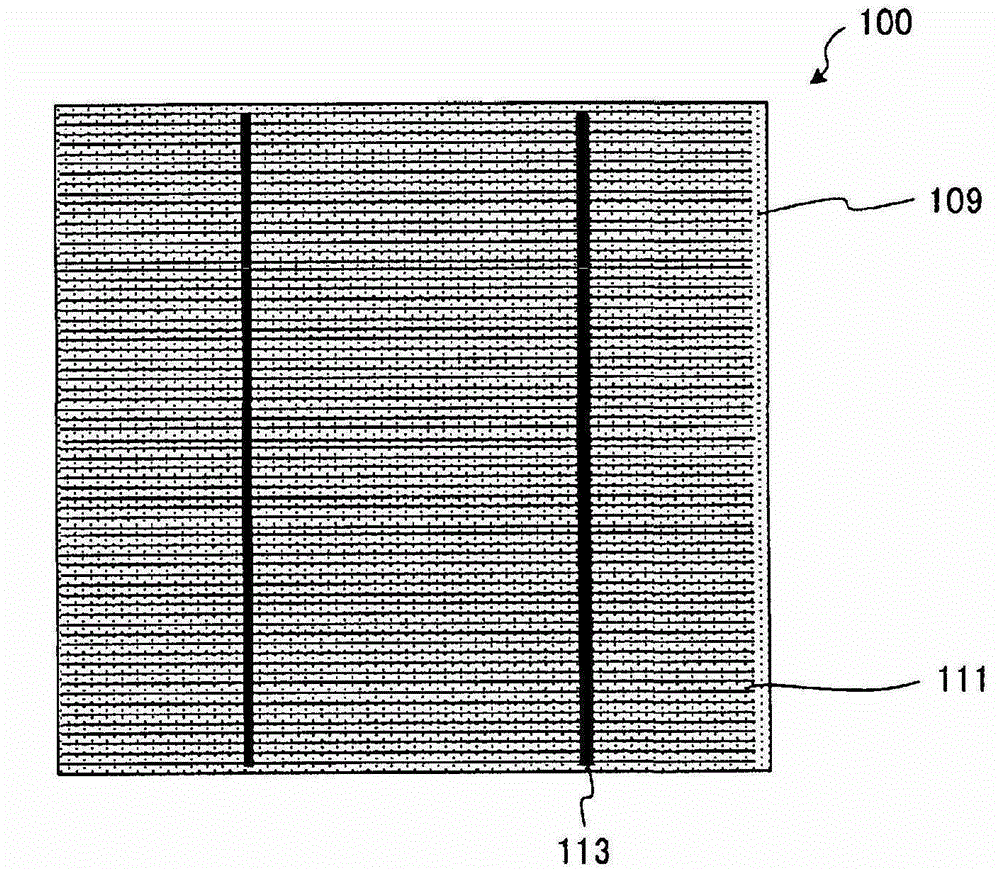
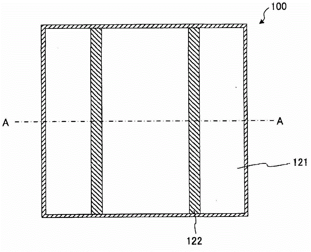
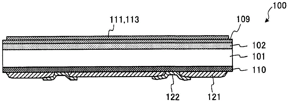
[0049] First, before explaining the structure of the photovoltaic device according to Embodiment 1 of the present invention, an outline of the overall structure of a general photovoltaic device will be described. FIGS. 1-1 to 1-3 are diagrams schematically showing an example of the overall structure of a general photovoltaic device. FIG. 1-1 is a plan view of the photovoltaic device, and FIG. 1-2 is a rear view of the photovoltaic device. , Figure 1-3 is a sectional view of AA of Figure 1-2. The photoelectromotive force device 100 is provided with a photoelectric conversion layer, and the photoelectric conversion layer includes: a P-type silicon substrate 101 as a semiconductor substrate; N-type impurity diffused layer 102 ; and P+ layer 110 containing P-type impurities at a higher concentration than silicon substrate 101 formed on the other main surface (rear surface) side. In addition, the photovoltaic device 100 includes: an anti-reflection film 109 that prevents reflectio...
Embodiment approach 2
[0076] In the description of Embodiment 1, after the high-resistance N-type diffusion layer 102H was formed in the concave portion 106 in FIGS. 5-7 and 6-7, the low-resistance N-type diffusion layer 102L and the high-resistance The phosphorous glass layer on the resistive N-type diffusion layer 102H can also be etched on the extreme surfaces of the low-resistance N-type diffusion layer 102L and the high-resistance N-type diffusion layer 102H with a mixed solution of hydrofluoric acid and nitric acid, for example. In addition, other processing steps are the same as those described in Embodiment 1, and therefore description thereof will be omitted.
[0077] According to Embodiment 2, after etching the phosphorus glass layer on the low-resistance N-type diffusion layer 102L and the high-resistance N-type diffusion layer 102H, these diffusion layers 102L are etched with a mixed acid such as a mixture of hydrofluoric acid and nitric acid. , The outermost surface of 102H is etched, ...
Embodiment approach 3
[0079] In this third embodiment, a case where openings are formed by a method different from that of the first embodiment will be described. Figure 9 It is a figure which shows an example of the structure of the laser processing apparatus used for opening formation in Embodiment 3. This laser processing apparatus 200B includes: a stage 201 on which a processing object such as a silicon substrate 101 is placed; a laser oscillator 203 that outputs a laser beam 204; The first galvano mirror 211 introduced into the optical path is scanned; and the second galvano mirror 213 introduced into the optical path while scanning the laser light 204 reflected by the first galvano mirror 211 in the Y-axis direction 214 .
[0080]In the laser processing apparatus 200B having such a structure, by scanning the first and second galvano mirrors 211 and 213, the laser light 204 converged in a point shape is irradiated to a predetermined position of the etching-resistant film 103 on the silicon su...
PUM
 Abstract
Description
Claims
Application Information
 - R&D
- Intellectual Property
- Life Sciences
- Materials
- Tech Scout
- Unparalleled Data Quality
- Higher Quality Content
- 60% Fewer Hallucinations
Browse by: Latest US Patents, China's latest patents, Technical Efficacy Thesaurus, Application Domain, Technology Topic, Popular Technical Reports.
© 2025 PatSnap. All rights reserved.Legal|Privacy policy|Modern Slavery Act Transparency Statement|Sitemap|About US| Contact US: help@patsnap.com


