A kind of method for making texture of solar cells
A technology for the surface of solar cells and silicon wafers, applied in the field of solar cells, can solve the problems of high suede reflectivity, many surface defects, difficult mass production, etc., and achieve the effects of simple process, few surface defects and low production cost
- Summary
- Abstract
- Description
- Claims
- Application Information
AI Technical Summary
Problems solved by technology
Method used
Image
Examples
Embodiment 1
[0032] (1) Add 50g of sodium silicate and 30g of carboxymethyl cellulose into 2kg of water, stir slowly until the two are completely dispersed; then add 1kg of silicon powder with a particle size of 2μm, and continue stirring for 5h until the silicon powder is evenly dispersed to obtain silicon slurry.
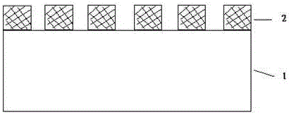
[0033] (2) Use the screen printing method to use the above mixed paste containing silicon powder, and the commercial specification is 156*156mm 2 The silicon paste prepared in step (1) was printed on the surface of the polycrystalline silicon wafer to form a silicon powder lattice with a dot diameter of 4 μm, a dot pitch of 2 μm, and a height of 10 μm, and dried in a chain oven at 80°C.
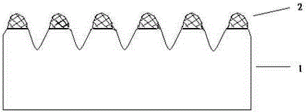
[0034] (3) Put the silicon wafer with a silicon powder lattice on the surface obtained in step (2) into an acidic etching solution at a temperature of 8°C for 4 minutes and chemically etch it. The acidic etching solution contains a volume ratio of HF:HNO 3 :H 2 The mixed system of O=1:4:1, ...
Embodiment 2
[0036] (1) Add 20g of orthosilicic acid and 5g of ethyl cellulose into 1kg of water, stir slowly until the two are completely dispersed; then add 1kg of silicon powder with a particle size of 15μm, and continue stirring for 5h until the silicon powder is evenly dispersed to obtain a silicon slurry material.
[0037] (2) Use the screen printing method to use the above mixed paste containing silicon powder, and the commercial specification is 156*156mm 2 The silicon paste prepared in step (1) was printed on the surface of the polycrystalline silicon wafer to form a silicon powder lattice with a dot diameter of 20 μm, a dot pitch of 5 μm, and a height of 30 μm, and dried in a chain oven at 80°C.
[0038] (3) Put the silicon wafer with a silicon powder lattice on the surface obtained in step (2) into an alkaline etching solution at a temperature of 50°C for 1 minute and chemically etch it for 1 minute. The alkaline etching solution is 8wt% KOH solution to obtain textured Wafer S2...
Embodiment 3
[0040] (1) Add 200g of silica gel and 100g of ethyl cellulose into 5kg of water, and stir slowly until the two are completely dispersed; then add 1kg of silicon powder with a particle size of 1 μm, and continue stirring for 5 hours until the silicon powder is evenly dispersed to obtain a silicon slurry.
[0041] (2) Use the screen printing method to use the above mixed paste containing silicon powder, and the commercial specification is 156*156mm 2 The silicon paste prepared in step (1) was printed on the surface of the polycrystalline silicon wafer to form a silicon powder lattice with a dot diameter of 1 μm, a dot pitch of 1 μm, and a height of 3 μm, and dried in a chain oven at 80°C.
[0042](3) Put the silicon wafer with a silicon powder lattice on the surface obtained in step (2) into an acidic etching solution at a temperature of 8°C for 4 minutes and chemically etch it. The acidic etching solution contains a volume ratio of HF:HNO 3 :H 2 The mixed system of O=1:4:1, th...
PUM
| Property | Measurement | Unit |
|---|---|---|
| particle diameter | aaaaa | aaaaa |
| particle diameter | aaaaa | aaaaa |
| particle diameter | aaaaa | aaaaa |
Abstract
Description
Claims
Application Information
 - R&D
- Intellectual Property
- Life Sciences
- Materials
- Tech Scout
- Unparalleled Data Quality
- Higher Quality Content
- 60% Fewer Hallucinations
Browse by: Latest US Patents, China's latest patents, Technical Efficacy Thesaurus, Application Domain, Technology Topic, Popular Technical Reports.
© 2025 PatSnap. All rights reserved.Legal|Privacy policy|Modern Slavery Act Transparency Statement|Sitemap|About US| Contact US: help@patsnap.com


