
Method for making glass substrate for display, glass substrate and display panel

A technology of glass substrate and manufacturing method, which is applied in the field of display panels, can solve problems such as TFT damage, peeling, and wiring pattern defects, and achieve the effect of suppressing static electricity and suppressing static electricity damage

Active Publication Date: 2013-10-30
AVANSTRATE INC
View PDF7 Cites 3 Cited by
  • Summary
  • Abstract
  • Description
  • Claims
  • Application Information

AI Technical Summary

Problems solved by technology

For example, when forming a TFT (Thin Film Transistor) and a wiring pattern on a glass substrate, impurities such as dust or dirt may adhere to the glass substrate or the wiring pattern due to static electricity, and the wiring pattern may be damaged or peeled off.
In addition, the TFT may be destroyed due to the discharge of the accumulated charge.
In addition, the glass substrate may adhere to the mounting table due to the above-mentioned static electricity, and when the glass substrate is removed from the mounting table, it may be broken.

Method used


Image

  • Method for making glass substrate for display, glass substrate and display panel
  • Method for making glass substrate for display, glass substrate and display panel
  • Method for making glass substrate for display, glass substrate and display panel

Examples


Embodiment

[0116] In order to examine the effect of this embodiment, the glass substrate for liquid crystal display devices using boroaluminosilicate glass was produced.

[0117] (rough surface treatment)

[0118] The above-mentioned atmospheric pressure plasma cleaning was performed on the produced glass substrate. That is, the plasma state of N 2 , O 2 The mixed gas flows to the entire width of the glass substrate at a specified amount per minute to clean the glass surface of the glass substrate.

[0119] Further, use Image 6 The etching apparatus 30 shown performs etching. In the etching device 30, the etching is performed by flowing a radicalized etching gas HF, which makes CF 4 、H 2 The mixed gas of O is obtained in plasma generated using a rare gas or the like.

[0120] Samples 1 to 8 shown in Table 1 below are for CF 4 、H 2 The supply of O, and the addition to CF 4 、H 2 The type of carrier gas in the mixed gas of O (N 2 or Ar gas) to variously change the shape of the ...


PUM

PropertyMeasurementUnit
heightaaaaaaaaaa
thicknessaaaaaaaaaa
surface roughnessaaaaaaaaaa

Abstract

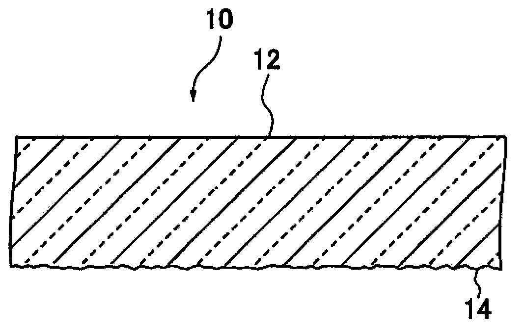
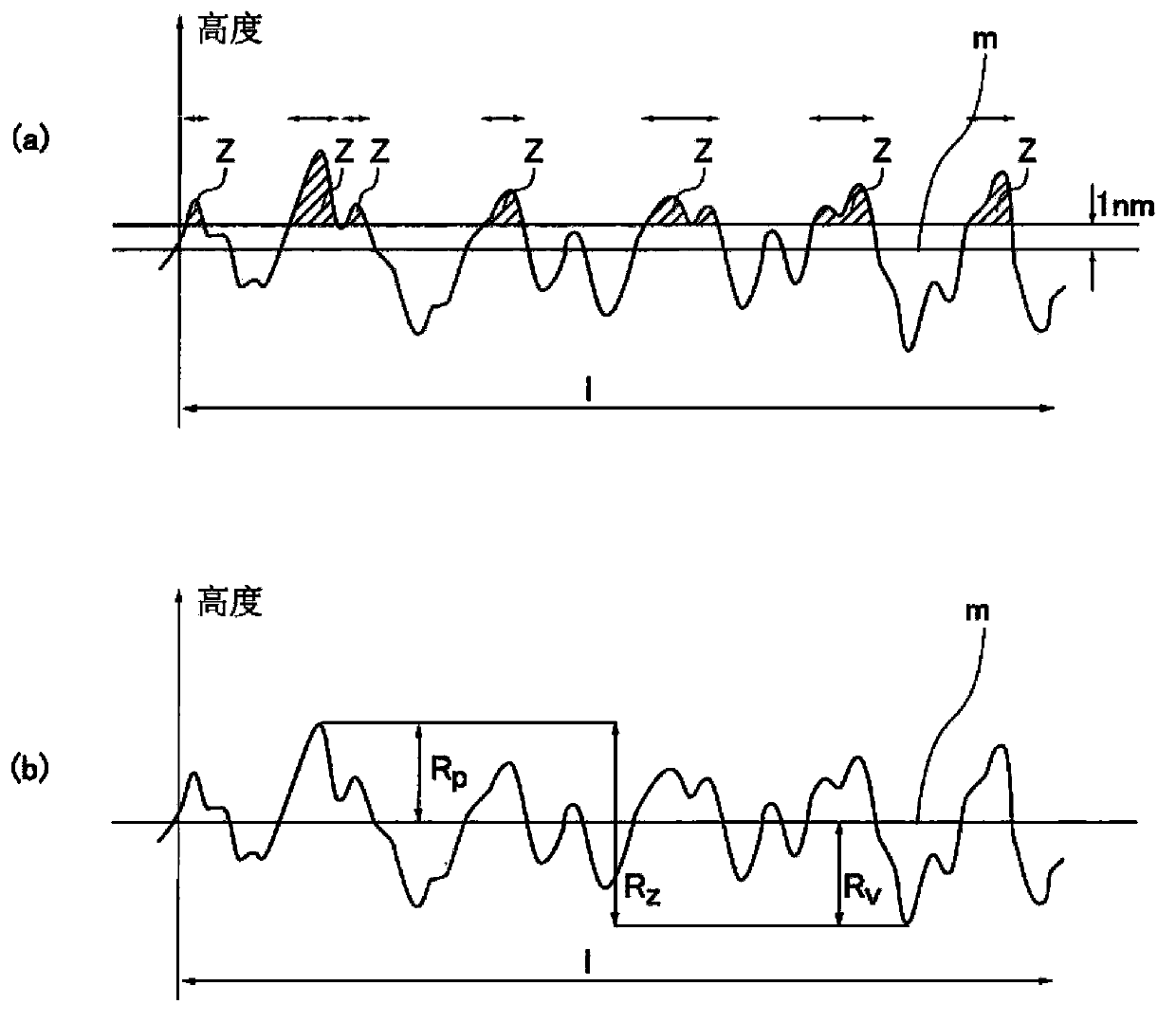
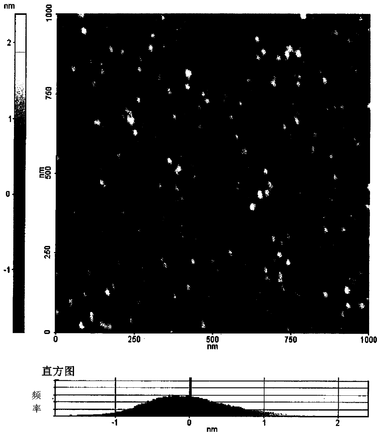
The invention provides a method for making a glass substrate for a display, a glass substrate and a display panel. The method for manufacturing a glass substrate for a display includes a step of producing a glass substrate and a step of performing a surface treatment on one glass surface of major surfaces of the glass substrate to form surface unevenness. The surface treatment is performed such that protruded portions having a height of 1 nm or more from the surface roughness central plane of the surface unevenness are dispersedly provided on the glass surface after the surface treatment and the area ratio of the protruded portions with respect to the area of the glass surface is 0.5-10%. Using this glass substrate, semiconductor elements are formed on a major surface of the glass substrate opposite to the glass surface. Accordingly, a display panel is produced.

Description

technical field [0001] This invention relates to the manufacturing method of the glass substrate for displays used for flat panel displays, such as a liquid crystal display, a plasma display, and an organic electroluminescent display, a glass substrate, and a panel for displays. Background technique [0002] Conventionally, in the manufacture of a flat panel display using a liquid crystal display panel, a plasma display panel, or an organic EL display panel used as a display panel, an exposure device is used to form a fine film on a glass substrate by photolithography. film pattern. [0003] The display panels used for these flat panel displays are produced after putting glass substrates into the production line, and then undergoing various processes such as transportation, film formation, photolithography, etching, doping, and wiring. In each process, the panel including the glass substrate is in an environment where static electricity is likely to be generated due to vari...

Claims


Application Information

Patent Timeline
Patent Type & Authority Applications(China)
IPC IPC(8): C03C15/00
Inventor 朴永太
Owner AVANSTRATE INC
Learn More