
Application of tapered nanometer optical fiber, and micro-fluidic chip and preparation method thereof

A microfluidic chip and nano-fiber technology, applied in the fields of chemistry and biology, can solve the problems of reducing the integration of the detection system, interfering with the fluorescent signal, affecting the sensitivity and reliability of sample detection, and improving the sensitivity and reliability. The effect of large surface and avoiding interference

Active Publication Date: 2013-10-09
HUAQIAO UNIVERSITY
View PDF1 Cites 3 Cited by
  • Summary
  • Abstract
  • Description
  • Claims
  • Application Information

AI Technical Summary

Problems solved by technology

However, for the microfluidic chip whose microchannel size is further reduced, the traditional method of direct laser irradiation or the method of embedding optical fibers in the chip will interfere with the large size of the fluorescence excitation device and the large illumination surface. The fluorescence signal of the sample in the microchannel affects the detection sensitivity and reliability of the sample; in addition, the direct irradiation excitation method separates the fluorescence excitation device and the microfluidic chip into two independent experimental units, which greatly reduces the overall application cost. The integration level of the detection system of the microfluidic chip

Method used


Image

  • Application of tapered nanometer optical fiber, and micro-fluidic chip and preparation method thereof
  • Application of tapered nanometer optical fiber, and micro-fluidic chip and preparation method thereof
  • Application of tapered nanometer optical fiber, and micro-fluidic chip and preparation method thereof

Examples


Embodiment Construction

[0033] In the following, the technical solutions of the present invention are further explained in detail through specific examples.

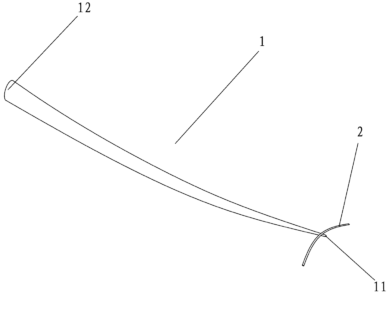
[0034] The application of a kind of tapered nanofiber of the present invention, as Figure 1-3 Prepare a smooth tapered nanofiber 1 as shown.

[0035] A smooth tapered nano-fiber 1 is extended from the tapered tip 11 into the microchannel 31 of the microfluidic chip substrate 3 as an optical waveguide for introducing the excitation light of fluorescence of the detected object. In a specific application, the excitation light of fluorescence is irradiated from the thick end 12 of the nanofiber 1, and the nanofiber 1 will guide the excitation light into the microchannel 31 and concentrate it on the cone tip 11 for emission. Since the excitation light is formed outside the nanofiber 1 Obvious evanescent field, and the cone tip 11 has an enhancement effect, so that the light intensity at the cone tip 11 increases significantly, and a sub-wavelength...


PUM


Abstract

The invention brings forward application of a tapered nanometer optical fiber. The smooth tapered nanometer optical fiber extends into a micro-channel of a micro fluidic chip substrate from a taper tip and is used as an optical waveguide for introduction of fluorescence exciting light of a to-be-detected object. According to a technical scheme provided by the invention, the tapered nanometer optical fiber is applied as the optical waveguide for introduction of fluorescence exciting light of the to-be-detected object, the taper tip of the nanometer optical fiber is inserted into the micro-channel of the micro fluidic chip substrate and corresponds to a designated to-be-detected point, the fluorescence exciting light irradiates and enters from a larger end of the nanometer optical fiber, and the nanometer optical fiber introduces the exciting light into the micro-channel and allows the exciting light to converge and then be shot out from the taper tip; fixed-point fluorescence excitation is carried out on the designated to-be-detected point, so interference of the exciting light on a fluorescence signal of a sample can be effectively avoided, and detection sensitivity and reliability are improved. The invention further brings forward a micro-fluidic chip and a preparation method thereof. The micro-fluidic chip not only has improved detection sensitivity and reliability but also enhances the integration level of a fluorescence excitation apparatus and the chip. The preparation method is simple, direct and highly efficient.

Description

technical field [0001] The invention relates to a microfluidic chip detection technology using a laser to excite fluorescence of a substance in the fields of biology and chemistry, and in particular to an application method of a tapered nanofiber, a microfluidic chip and a preparation method thereof. Background technique [0002] It is an important biochemical detection method to use laser to excite the fluorescence of the detection substance and analyze the composition and concentration of the sample. Microfluidic chips can integrate basic operating units such as sample preparation, biochemical reactions, separation, and detection in the fields of biology and chemistry on centimeter-scale chips. [0003] In recent years, in the field of microfluidics, with the continuous improvement of the requirements of microfluidics technology, the size of microchannels of microfluidics chips has been gradually reduced. However, for the microfluidic chip whose microchannel size is furth...

Claims


Application Information

Patent Timeline
IPC IPC(8): G01N21/61B01L3/00
Inventor 张奚宁童利民戴昊胡志方
Owner HUAQIAO UNIVERSITY
Learn More