Heat shield of polysilicon CVD (chemical vapor deposition) reactor
A technology for reactors and heat shields, which is applied in the field of energy-saving devices, can solve the problems of low deposition rate and single furnace output, large heat radiation of quartz bell jars, and difficult to enlarge the size, so as to reduce processing difficulty and maintenance costs, reduce The effect of maintenance frequency and reducing the risk of release
- Summary
- Abstract
- Description
- Claims
- Application Information
AI Technical Summary
Problems solved by technology
Method used
Image
Examples
Embodiment 1
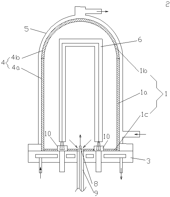
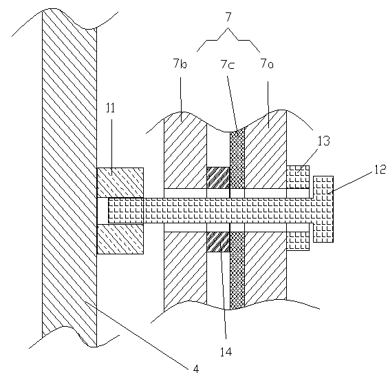
[0026] Such as figure 1 , figure 2 As shown, using the same reduction furnace, a double-layer quartz glass heat shield 1 is placed between the inner wall of a polysilicon CVD reactor 2 and the outermost polysilicon rod 6 in the reactor and fixed on the inner wall 4 of the furnace cylinder. The thickness of layer quartz glass 7a, 7b is 5-15mm, and the spacer between two layers of glass adopts graphite spacer 14, and outer layer quartz glass 7a is coated with silver or gold back reflection layer 7c, and the silver or gold back reflection layer The thickness is about 0.5-3 μm, and the furnace cylinder side wall 4a is covered with quartz glass 1a, and the furnace cylinder dome 4b and the bottom plate 3 are not covered. The CVD reactor is fed with a mixed gas of trichlorosilane and hydrogen, using the same molar ratio, reaction temperature and pressure as the comparative example, and the silicon rod is grown from a diameter of 8mm to about 120mm, repeated 3 times, and the avera...
Embodiment 2
[0028] On the basis of embodiment 1, covered dome 4b with quartz glass 1b, furnace drum dome adopts such as image 3 The splicing shown does not cover chassis 3. The CVD reactor is fed with a mixed gas of trichlorosilane and hydrogen, using the same molar ratio, operating pressure and reaction temperature as the comparative example, the silicon rod is grown from a diameter of 8mm to about 120mm, repeated 3 times, and the average deposition power consumption is 47kWh / kg-Si, the average deposition time is 73h, and the electrical parameters of the product meet the requirements of the national standard GB / T12963-2009 silicon polycrystalline secondary standard.
Embodiment 3
[0030] On the basis of Example 2, the cover chassis 3 is covered with quartz glass 1c. The CVD reactor is fed with a mixed gas of trichlorosilane and hydrogen, using the same molar ratio, operating pressure and reaction temperature as the comparative example, the silicon rod is grown from a diameter of 8mm to about 120mm, repeated twice, and the average deposition power consumption is 42kWh / kg-Si, the average deposition time is 71h, and the electrical parameters of the product meet the requirements of the national standard GB / T12963-2009 silicon polycrystalline secondary standard. Can find out from the comparison of embodiment 1,2,3 and comparative example, adopt heat shield can substantially save electric energy, and shorten deposition time and make the output in unit time be promoted, and product quality does not have obvious change.
PUM
| Property | Measurement | Unit |
|---|---|---|
| thickness | aaaaa | aaaaa |
| thickness | aaaaa | aaaaa |
| melting point | aaaaa | aaaaa |
Abstract
Description
Claims
Application Information
 - R&D
- Intellectual Property
- Life Sciences
- Materials
- Tech Scout
- Unparalleled Data Quality
- Higher Quality Content
- 60% Fewer Hallucinations
Browse by: Latest US Patents, China's latest patents, Technical Efficacy Thesaurus, Application Domain, Technology Topic, Popular Technical Reports.
© 2025 PatSnap. All rights reserved.Legal|Privacy policy|Modern Slavery Act Transparency Statement|Sitemap|About US| Contact US: help@patsnap.com


