Infrared thermopile sensor based on cmos DPTM process and its manufacturing method
A manufacturing method and technology of thermopile, applied to the process for producing decorative surface effects, electric solid devices, electric radiation detectors, etc., can solve the problems of high manufacturing cost, large chip size, poor process compatibility, etc., and achieve manufacturing Low cost, reduced resistance thermal noise, and improved detection rate
- Summary
- Abstract
- Description
- Claims
- Application Information
AI Technical Summary
Problems solved by technology
Method used
Image
Examples
Embodiment 1
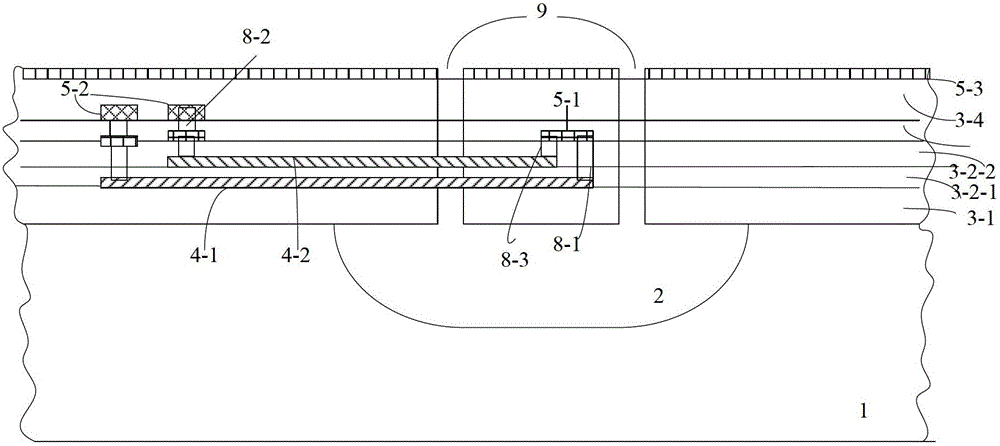
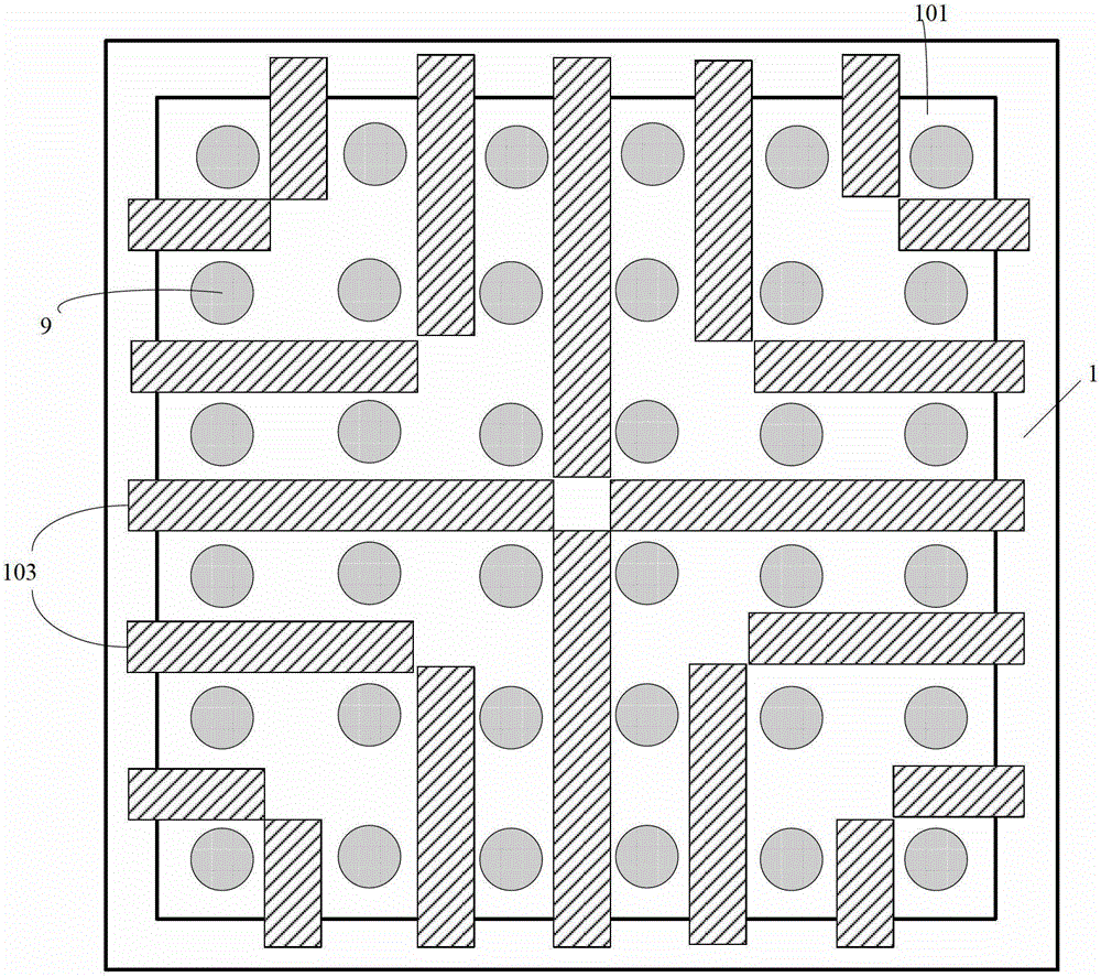
[0055] Such as figure 1 , image 3 As shown: the infrared thermopile sensor includes a silicon substrate 1 and a closed film region 101 located on the silicon substrate 1. The closed film region 101 is sequentially composed of a first dielectric layer 3-1 and a second dielectric layer 3-2 from the bottom up. , the third dielectric layer 3-3 and the fourth dielectric layer 3-4, the first polysilicon layer 4-1 is set between the first dielectric layer 3-1 and the second dielectric layer 3-2, and the second dielectric layer A first metal layer 5-1 is arranged between the layer 3-2 and the third dielectric layer 3-3, and a second metal layer 5-2 is arranged between the third dielectric layer 3-3 and the fourth dielectric layer 3-4, The third metal layer 5-3 is provided on the surface of the fourth dielectric layer 3-4; the first through hole 8-1 and the second via hole 8-1 are respectively provided on the second dielectric layer 3-2 and the third dielectric layer 3-3. Through ho...
Embodiment 2
[0072] Such as figure 2 , image 3 As shown: the infrared thermopile sensor includes a silicon substrate 1 and a closed film region 101 located on the silicon substrate 1. The closed film region 101 is sequentially composed of a first dielectric layer 3-1 and a second dielectric layer 3-2 from the bottom up. , the third dielectric layer 3-3 and the fourth dielectric layer 3-4, the first polysilicon layer 4-1 is set between the first dielectric layer 3-1 and the second dielectric layer 3-2, and the second dielectric layer A first metal layer 5-1 is arranged between the layer 3-2 and the third dielectric layer 3-3, and a second metal layer 5-2 is arranged between the third dielectric layer 3-3 and the fourth dielectric layer 3-4, A third metal layer 5-3 is provided on the surface of the fourth dielectric layer 3-4; the second dielectric layer 3-2 is composed of a first layer of silicon oxide 3-2-1 and a second layer of silicon oxide 3-2-2 Composition, the second polysilicon l...
PUM
| Property | Measurement | Unit |
|---|---|---|
| thickness | aaaaa | aaaaa |
| thickness | aaaaa | aaaaa |
| length | aaaaa | aaaaa |
Abstract
Description
Claims
Application Information
 - R&D
- Intellectual Property
- Life Sciences
- Materials
- Tech Scout
- Unparalleled Data Quality
- Higher Quality Content
- 60% Fewer Hallucinations
Browse by: Latest US Patents, China's latest patents, Technical Efficacy Thesaurus, Application Domain, Technology Topic, Popular Technical Reports.
© 2025 PatSnap. All rights reserved.Legal|Privacy policy|Modern Slavery Act Transparency Statement|Sitemap|About US| Contact US: help@patsnap.com


