Microcrystalline semiconductor thin film production process

A thin-film manufacturing method and technology for microcrystalline semiconductors, which are applied in the manufacturing of semiconductor/solid-state devices, semiconductor devices, gaseous chemical plating, etc., can solve the problems of internal oxidation, adverse effects of solar cell characteristics, surface oxidation, etc., and achieve uniform crystallization efficiency, high performance, and low cost

Inactive Publication Date: 2013-08-14
MITSUBISHI ELECTRIC CORP
View PDF4 Cites 0 Cited by
  • Summary
  • Abstract
  • Description
  • Claims
  • Application Information

AI Technical Summary

Problems solved by technology

Thus, in the microcrystalline silicon thin film obtained by the conventional method, there is a problem that not only the surface of the film is oxidized, but also the inside of the film is oxidized, or it is contaminated with impurities such as carbon, which adversely affects the characteristics of the solar cell.

Method used


Image

  • Microcrystalline semiconductor thin film production process
  • Microcrystalline semiconductor thin film production process
  • Microcrystalline semiconductor thin film production process

Examples


Embodiment approach 1

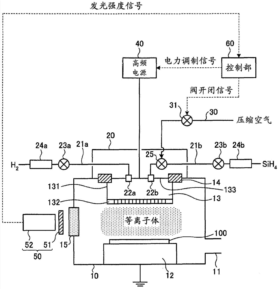
[0034] figure 1 It is a diagram schematically showing an example of the structure of the microcrystalline semiconductor thin film manufacturing apparatus according to Embodiment 1 of the present invention. This microcrystalline semiconductor thin film manufacturing apparatus is based on a conventional plasma CVD apparatus, and includes a substrate stage 12 and a plasma electrode 13 in a vacuum chamber 10 in which an atmosphere for forming a semiconductor thin film is formed, and is provided as the plasma electrode 13. The surfaces facing the substrate stage 12 are parallel to each other. In the vacuum container 10, a gas exhaust pipe 11 is provided, and the gas in the vacuum container 10 is exhausted by an unillustrated vacuum pump connected to the gas exhaust pipe 11, and the inside of the vacuum container 10 is set to a predetermined value. Vacuum.

[0035] The substrate stage 12 is electrically grounded, and has a structure on which the substrate 100 to be subjected to th...

Embodiment approach 2

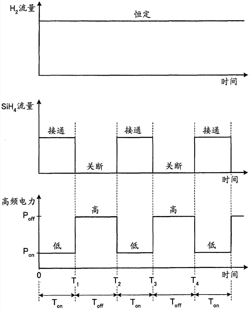
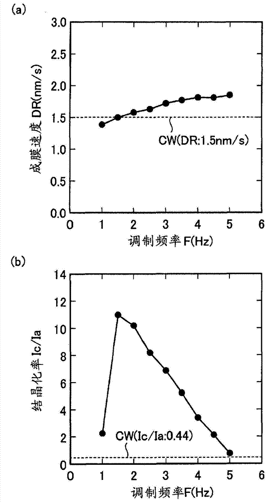
[0091] In the above-mentioned Example 1, it was explained that the SiH 4 The duty cycle R of the on / off modulation of the gas supply becomes constant so that the SiH 4 The frequency F of the ON / OFF modulation of the gas supply is changed over time to form a film, but on the contrary even if the SiH 4 The frequency F of the on / off modulation of the gas supply becomes constant such that the SiH 4 Varying the duty ratio R of the on / off modulation of the gas supply over time can also improve the uniformity of crystallinity. In Embodiment 2, it is specified that the figure 1 An example in which the duty ratio R is changed in the initial stage of film formation of the microcrystalline silicon thin film in the microcrystalline semiconductor thin film manufacturing apparatus shown.

[0092] Using the microcrystalline semiconductor thin film manufacturing method (SiH 4 In the microcrystalline silicon thin film of the gas pulse method), for example, the high-frequency power is turne...


PUM


Abstract

A microcrystalline semiconductor thin film production process comprises a microcrystalline semiconductor thin film formation step of intermittently supplying a semiconductor material gas containing at least silicon or germanium to a vacuum container equipped with a plasma electrode and a substrate while continuously supplying a gas containing hydrogen as the main component, synchronizing a period during which the semiconductor material gas is supplied with a period during which the semiconductor material gas is not supplied, and supplying different high-frequency electric powers to the plasma electrode to generate plasma in a plasma generation space that is located between the plasma electrode and the substrate, thereby forming the microcrystalline semiconductor thin film, wherein, in the microcrystalline semiconductor thin film formation step, the on / off modulation of the supply of the semiconductor material gas is carried out to supply the semiconductor material gas periodically, the high-frequency electric power that is used during the turning-on of the supply of the semiconductor material gas is smaller than a high-frequency electric power that is used during the turning-off of the supply of the semiconductor material gas, and the modulation frequency of the on / off modulation or the duty ratio of the on / off modulation is altered over time.

Description

technical field [0001] The present invention relates to a method for producing a microcrystalline semiconductor thin film, and more particularly to a method for producing a microcrystalline semiconductor thin film of microcrystalline silicon, microcrystalline silicon germanium, or the like used in a photoelectric conversion layer of a silicon-based thin film solar cell. Background technique [0002] As one type of photoelectric conversion layer of a silicon-based thin-film solar cell, for example, a microcrystalline silicon thin film is widely used. As a method of manufacturing this microcrystalline silicon film, generally, by using silane (SiH 4 ) and hydrogen (H 2 ) plasma CVD (Chemical Vapor Deposition, chemical vapor deposition) method of a mixed gas is deposited on a glass substrate at a low temperature (˜200° C.) (for example, refer to Patent Document 1, Non-Patent Document 1). [0003] In a plasma CVD apparatus, a plasma electrode that generates discharge plasma and...

Claims


Application Information

Patent Timeline
IPC IPC(8): H01L21/205H01L31/04
CPCH01L21/02532C23C16/24C23C16/505H01L31/1816C23C16/45523H01L21/0262Y02E10/50
Inventor 津田睦今村谦滝正和池田知弘藤原伸夫
Owner MITSUBISHI ELECTRIC CORP
Why Eureka
Try Eureka