Enclosed and grooved type power semiconductor component and manufacturing method thereof

A technology of power semiconductors and manufacturing methods, which is applied in the direction of semiconductor devices, electrical components, circuits, etc., and can solve problems affecting critical voltage values, etc.

Inactive Publication Date: 2013-08-14
SUPER GROUP SEMICON
View PDF5 Cites 0 Cited by
  • Summary
  • Abstract
  • Description
  • Claims
  • Application Information

AI Technical Summary

Problems solved by technology

Therefore, the dopant in the heavily doped region 16' is easy to diffuse to the side of the trench gate structure 12' due to the subsequent thermal process, and the diffused region is shown by the dotted line, changing the doping concentration at the channel. , which in turn affects the threshold voltage set by the original power semiconductor components (threshold voltage)

Method used


Image

  • Enclosed and grooved type power semiconductor component and manufacturing method thereof
  • Enclosed and grooved type power semiconductor component and manufacturing method thereof
  • Enclosed and grooved type power semiconductor component and manufacturing method thereof

Examples


Embodiment Construction

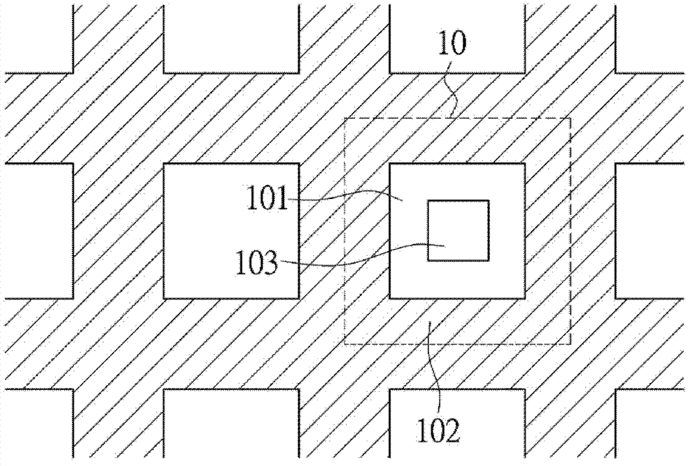
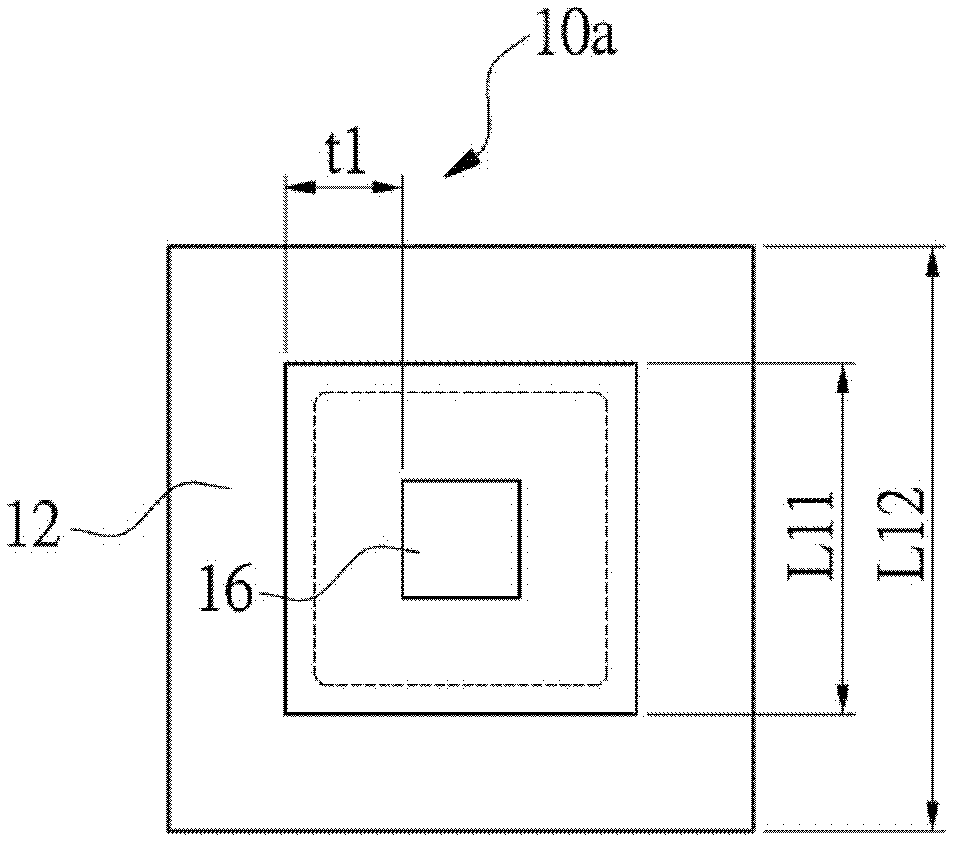
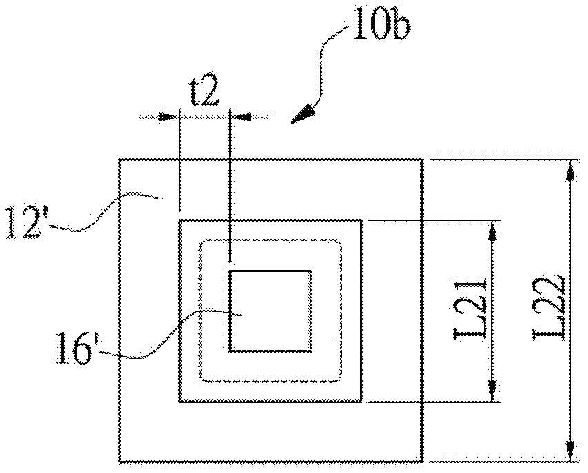
[0063] figure 2 It is an embodiment of the closed trench power semiconductor element of the present invention. like figure 2 As shown, the closed trench power semiconductor device 20 includes a substrate 21 and a plurality of unit cells 20a, and the unit cells 20a are arranged in the substrate 21 in an array.

[0064] Figure 2A for figure 2 A schematic diagram of a unit cell 20a of a closed trench power semiconductor device. like Figure 2A As shown, the unit cell 20a includes a body region 24 and a trench gate 22, and has a square shape. Wherein, the trench gate 22 surrounds the body region 24 and defines the shape of the body region 24 . The source doped region is adjacent to the trenched gate 22 . The center of the body region 24 also has a heavily doped region 26 . There is a dielectric pattern layer above the body region 24 and the trenched gate 22 , and a source contact window 25 is defined inside to expose the source doped region and the heavily doped region...


PUM


Abstract

The invention relates to an enclosed and grooved type power semiconductor component and a manufacturing method thereof. The enclosed and grooved type power semiconductor component comprises a substrate material and a plurality of unit cells, wherein the plurality of the unit cells are arranged inside the substrate material in group; each unit cell comprises a body area and a grooved type grid; the grooved type grid surrounds the periphery of the body area; and at least one side wall of the grooved type is provided with a recess on the side facing towards the body area. The enclosed and grooved type power semiconductor component provided by the invention can maintain the improvement of passage width of unit area after line width reduction, while avoiding a possible negative influence on a critical voltage value after line width reduction.

Description

technical field [0001] The invention relates to a trench type power semiconductor element and a manufacturing method thereof, in particular to a closed cell trench type power semiconductor element and a manufacturing method thereof. Background technique [0002] The structure of the trench power semiconductor device can be divided into closed cell and striped cell, and the main difference between the two lies in the distribution of the trench gate structure. For the elongated trench-type power semiconductor element, the trench-type gate structure is elongated and equidistantly distributed in the body layer of the trench-type power semiconductor element. For the closed trench power semiconductor device, the trench gate structure is distributed in the body layer of the trench power semiconductor device in a network shape, and defines a plurality of square regions in the body layer. Compared with elongated trench power semiconductor elements, closed trench power semiconductor ...

Claims


Application Information

Patent Timeline
IPC IPC(8): H01L29/423H01L21/28H01L29/78
Inventor 张渊舜涂高维蔡依芸
Owner SUPER GROUP SEMICON
Why Eureka
Try Eureka