


Quick Research
Generate reliable direction feasibility study reports for your R&D in just a few steps.

Technical Q&A
Discover and master advanced knowledge NOW. Basics, ideas, possibilities, all at once.

Find Solutions
As an expert in R&D theories, this can generate solutions to your technical problems instantly.

Evaluate Feasibility
Analyze your overall solution with one click, know your potential R&D risks in advance.

Monitor Landscape
Get weekly tech updates, stay abreast of the latest tech innovations and key insights.
ITO-indium halide bilayer conductive film and preparation method thereof
A technology of indium halide and conductive film, which is applied in coatings, electric light sources, electrical components, etc., can solve the problems of increasing carrier injection barriers, affecting the conductivity of thin films, and hindering luminous efficiency, so as to achieve work function improvement and luminescence Efficiency-enhancing, easy-to-control effects
- Summary
- Abstract
- Description
- Claims
- Application Information
AI Technical Summary
Problems solved by technology
Method used
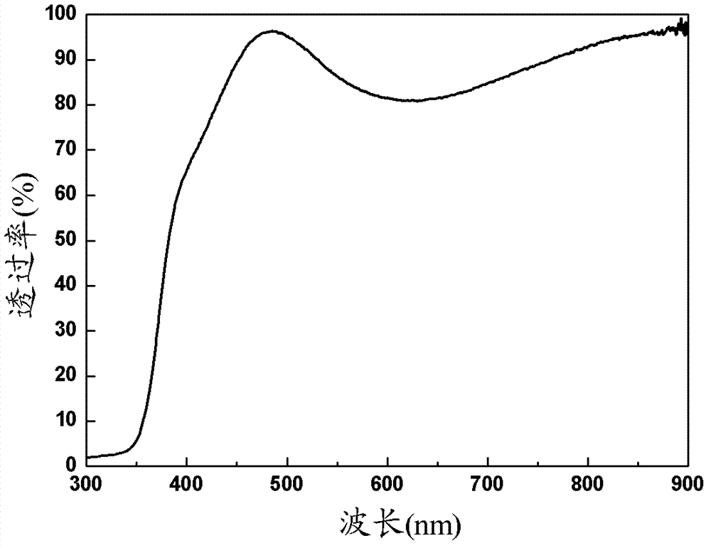
Image

Examples
Embodiment 1
[0025] 1. Select In with a purity of 99.99% 2 o 3 and SnO 2 Powder (of which, In 2 o 3 The mass number is 176g, SnO 2 The mass number is 24g), after uniform mixing, sintering at 1250°C, and natural cooling to obtain an ITO ceramic target sample, which is cut into an ITO ceramic target with a diameter of 50 mm and a thickness of 2 mm; and
[0026] Choose InF with a purity of 99.99% 3 Powder 150g, sintered at 750°C, cooled naturally to obtain InF 3 Ceramic target sample, cut the ceramic target sample into InF with a diameter of 50mm and a thickness of 2mm 3 ceramic target;
[0027] 2. Combine ITO, InF 3 The ceramic target is loaded into the vacuum chamber of the magnetron sputtering coating equipment;
[0028] 3. Clean the glass substrate ultrasonically with acetone, absolute ethanol and deionized water successively, and perform oxygen plasma treatment on it, and then put it into the vacuum chamber of the magnetron sputtering coating equipment; among them, the substrate...
Embodiment 2
[0034] 1. Select In with a purity of 99.99% 2 o 3 and SnO 2 Powder (of which, In 2 o 3 The mass number is 194g, SnO 2 The mass number is 6g), after uniform mixing, sintering at 900°C, and natural cooling to obtain an ITO ceramic target sample, which is cut into an ITO ceramic target with a diameter of 50 mm and a thickness of 2 mm; and
[0035] Choose InF with a purity of 99.99% 3 150g powder, sintered at 600°C, cooled naturally to obtain InF 3 Ceramic target sample, cut the ceramic target sample into InF with a diameter of 50mm and a thickness of 2mm 3 ceramic target;
[0036] 2. Combine ITO, InF 3The ceramic target is loaded into the vacuum chamber of the magnetron sputtering coating equipment;
[0037] 3. Clean the glass substrate ultrasonically with acetone, absolute ethanol and deionized water successively, and perform oxygen plasma treatment on it, and then put it into the vacuum chamber of the magnetron sputtering coating equipment; among them, the substrate of...
Embodiment 3
[0042] 1. Select In with a purity of 99.99% 2 o 3 and SnO 2 Powder (of which, In 2 o 3 The mass number is 160g, SnO 2 The mass number is 40g), after uniform mixing, sintering at 1300°C, and natural cooling to obtain an ITO ceramic target sample, which is cut into an ITO ceramic target with a diameter of 50mm and a thickness of 2mm; and
[0043] Choose InF with a purity of 99.99% 3 Powder 150g, sintered at 950°C, cooled naturally to obtain InF 3 Ceramic target sample, cut the ceramic target sample into InF with a diameter of 50mm and a thickness of 2mm 3 ceramic target;
[0044] 2. Combine ITO, InF 3 The ceramic target is loaded into the vacuum chamber of the magnetron sputtering coating equipment;
[0045] 3. Clean the glass substrate ultrasonically with acetone, absolute ethanol and deionized water successively, and perform oxygen plasma treatment on it, and then put it into the vacuum chamber of the magnetron sputtering coating equipment; among them, the substrate o...
PUM
| Property | Measurement | Unit |
|---|---|---|
| Block resistance | aaaaa | aaaaa |
| Surface work function | aaaaa | aaaaa |
| Block resistance | aaaaa | aaaaa |
Abstract
Description
Claims
Application Information
 - R&D Engineer
- R&D Manager
- IP Professional
- Industry Leading Data Capabilities
- Powerful AI technology
- Patent DNA Extraction
Browse by: Latest US Patents, China's latest patents, Technical Efficacy Thesaurus, Application Domain, Technology Topic, Popular Technical Reports.
© 2024 PatSnap. All rights reserved.Legal|Privacy policy|Modern Slavery Act Transparency Statement|Sitemap|About US| Contact US: help@patsnap.com