
Solid electrolytic capacitor element, its manufacturing method and its manufacturing tool

A technology of solid electrolysis and manufacturing method, applied in the direction of electrolytic capacitor manufacturing, solid electrolytic capacitor, capacitor manufacturing, etc., can solve the problems of rising, corrosion and deterioration of the dielectric layer, etc. Effect

Inactive Publication Date: 2015-11-25
RESONAC HOLDINGS CORPORATION
View PDF9 Cites 0 Cited by
  • Summary
  • Abstract
  • Description
  • Claims
  • Application Information

AI Technical Summary

Problems solved by technology

The result will exceed the standard of humidity test
In addition, if moisture penetrates into the dielectric layer portion in the pores of the anode body where the semiconductor is not impregnated, the probability of causing corrosion and deterioration of the dielectric layer increases.

Method used

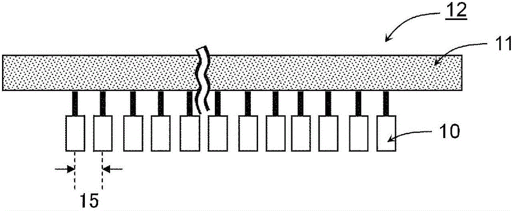
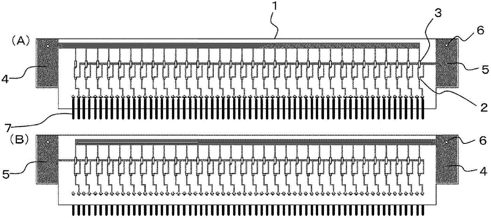
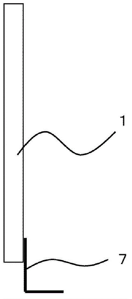

Image

  • Solid electrolytic capacitor element, its manufacturing method and its manufacturing tool
  • Solid electrolytic capacitor element, its manufacturing method and its manufacturing tool
  • Solid electrolytic capacitor element, its manufacturing method and its manufacturing tool

Examples


Embodiment 1~3 and comparative example 1~4

[0091] After the niobium ingot was stored hydrogen, it was pulverized, dehydrogenated, nitrided, and then granulated to obtain niobium powder with a CV of 150,000 μF·V / g and a nitrogen content of 8,600 ppm. The niobium powder is molded together with a niobium lead wire of 0.29 mmФ, and vacuum sintered at 1280 ° C for 30 minutes to obtain a size of 1.5 × 3.0 × 4.5 mm (volume is 20.25 mm) 3 ), the density is 3.3g / cm 3 There are 640 niobium sintered bodies, and these niobium sintered bodies are used as anode bodies. In addition, the niobium lead was implanted in the center of the 1.5×3.0 mm surface so that 3.7 mm was buried inside the sintered body and 4.3 mm was exposed on the outer surface.

[0092] A separately prepared spacer made of tetrafluoroethylene polymer having an outer diameter of 2 mm, an inner diameter of 0.26 mm, and a thickness of 0.2 mm was inserted into the lead wire at a position 0.2 mm from the surface of the sintered body.

[0093] Next, connect the front e...

Embodiment 4~5 and comparative example 5~6

[0108] In the same manner as in Example 1, niobium powder with a CV value of 220,000 μF·V / g and a nitrogen content of 15,000 ppm was prepared by adjusting the pulverization time and nitriding treatment time to obtain a sintered body. About this niobium sintered body (1.0×2.4×3.4mm (volume 8.16mm 3 ) except that the electrolytic polymerization conditions were set to the values ​​shown in Table 2, a capacitor element was produced in the same manner as in Example 1, and the capacity of the obtained capacitor element was measured to obtain the impregnation rate. The results are shown in Table 2. In addition, Table 5 shows the average capacity of the capacitors produced in the same manner as in Example 1 and the range of the upper and lower limit values ​​of the capacity.

[0109] Table 2

[0110]

Embodiment 6~7 and comparative example 7~8

[0112] In Example 1, commercially available tantalum powder CV 70,000 μF·V / g was used instead of niobium powder. The tantalum powder was vacuum sintered at 1400°C for 30 minutes to obtain a density of 6.5g / cm 3 , size 2.5×3.8×7.2mm (volume 68.4mm 3 ) of the sintered body. Furthermore, on the sintered body, a tantalum lead with a diameter of 0.40 mmФ was planted on the 2.5×3.8 mm surface of the sintered body.

[0113] Capacitor elements were produced in the same manner as in Example 1 except that the conditions of electrolytic polymerization were set to the values ​​shown in Table 3, and the capacitance of the obtained capacitor elements was measured to obtain the impregnation rate. The results are shown in Table 3. In addition, Table 5 shows the average capacity of the capacitors produced in the same manner as in Example 1 and the range of the upper and lower limit values ​​of the capacity.

[0114] table 3

[0115]


PUM

PropertyMeasurementUnit
volumeaaaaaaaaaa
apparent porosityaaaaaaaaaa
densityaaaaaaaaaa

Abstract

The present invention relates to a method of manufacturing a solid electrolytic capacitor element comprising the steps of forming a semiconductor layer on the dielectric layer formed on surfaces of a plurality of anode bodies at one time, wherein a step of forming a semiconductor layer comprises repeating an electrolytic polymerization operation several times by applying a current from a power-feeding terminal that comes into contact with each anode body, and at least one of the electrolytic polymerization operations continuously applies a current while changing the amount of current between the range of 5 to 200 µA per power-feeding terminal; and a jig for electrolytic polymerization for forming a semiconductor layer on the dielectric layer formed on a surface of an anode body, comprising a plurality of power supply circuits (i) provided on an insulating substrate and capable of continuously changing the amount of current between a lower limit and an upper limit; and a power-feeding terminals (ii) electrically connected to the output of each of the plurality of power supply circuits to be placed in contact with anode bodies. According to the present invention, a group of capacitor elements having high humidity resistance can be obtained by forming a semiconductor layer at one time on the dielectric layer formed on a plurality of anode bodies by electrolytic polymerization with a high impregnation rate.

Description

technical field [0001] The present invention relates to a method of manufacturing a solid electrolytic capacitor element capable of realizing a stable capacity appearance ratio, a tool (jig) for electrolytic polymerization for forming a semiconductor layer of the solid electrolytic capacitor element, and the manufacturing method or tool using the same Fabricated solid electrolytic capacitor elements. Background technique [0002] A solid electrolytic capacitor has a conductor (anode body) as one electrode, and includes a dielectric layer formed on the surface of the electrode and the other electrode (semiconductor layer) provided on the dielectric layer. In the case of manufacturing a solid electrolytic capacitor in which the semiconductor layer is made of a conductive polymer, a dielectric layer is formed on the anode body by chemical conversion, and a semiconductor layer is sequentially formed by electrolytic polymerization. Generally, a plurality of anode bodies are elec...

Claims


Application Information

Patent Timeline
Patent Type & Authority Patents(China)
IPC IPC(8): H01G9/00H01G9/028H01G9/15H01G13/00
CPCH01G9/0029H01G9/0036H01G9/028H01G9/15H01G13/00
Inventor 内藤一美铃木雅博
Owner RESONAC HOLDINGS CORPORATION
Learn More