Method of eliminating etching residue of emitting electrode polycrystalline silicon in duotriode type transistor technology

A bipolar transistor and etching residue technology, which is applied in semiconductor/solid-state device manufacturing, electrical components, circuits, etc., can solve the problems of emitter polysilicon etching residue, etc., so as to solve the etching residue and reduce the risk of leakage , the effect of shortening the distance

Active Publication Date: 2013-05-08
SHANGHAI HUAHONG GRACE SEMICON MFG CORP
View PDF3 Cites 8 Cited by
  • Summary
  • Abstract
  • Description
  • Claims
  • Application Information

AI Technical Summary

Problems solved by technology

[0003] The technical problem to be solved by the present invention is to provide a method for removing polysilicon etching residues on the emitter in the process of bipolar transistors, which can solve the problem of polysilicon etching residues on the emitter and eliminate the possibility of base and collector leakage

Method used


Image

  • Method of eliminating etching residue of emitting electrode polycrystalline silicon in duotriode type transistor technology
  • Method of eliminating etching residue of emitting electrode polycrystalline silicon in duotriode type transistor technology
  • Method of eliminating etching residue of emitting electrode polycrystalline silicon in duotriode type transistor technology

Examples


Embodiment Construction

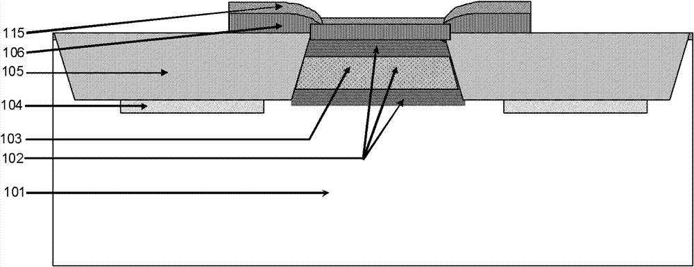
[0027] The bipolar transistor structure produced by the method for removing the emitter polysilicon etching residue in the bipolar transistor process in the present invention is as follows Figure 6 As shown, the active region consists of shallow trench field oxygen ie figure 1 The shallow trench isolation layer 105 in isolation includes a collector region, a pseudo-buried layer, a base region and an emitter region.

[0028] Such as Figure 1 to Figure 6 Shown is a schematic diagram of the device structure during the manufacturing process of the embodiment of the present invention. The method of the embodiment of the present invention, such as Figure 7 shown, including the following steps:

[0029] In step 1, a shallow trench isolation layer 105 is formed on the P-type silicon substrate 101, and a dose of 10 is implanted at the bottom of the shallow trench isolation layer 105. 15 ~10 16 cm -2 N-type ions with an energy of 5-15keV form the N-type pseudo-buried layer 104...


PUM

PropertyMeasurementUnit
thicknessaaaaaaaaaa

Abstract

The invention discloses a method of eliminating etching residues of emitting electrode polycrystalline silicon in duotriode type transistor technology. A base region germanium-silicon outer extension layer is developed. A layer of an oxidation film is developed on the base region germanium-silicon outer extension layer. The oxidation film and the germanium-silicon outer extension layer are etched through a drying method, thus a base electrode of the duotriode type transistor is formed. The oxidation film on the base electrode can be clearly eliminated by using the drying method. A medium film is deposited by the composition of the oxidation film and a nitride film. The medium film is etched, thus an emitting electrode window is formed. The emitting electrode polycrystalline silicon is deposited and an ion is injected. The emitting electrode is formed by etching. End surfaces on two sides of an outer base region polycrystalline silicon are filled by the medium layer forming the emitting electrode window, thus the residue on two sides of the base electrode polycrystalline silicon when the emitting electrode polycrystalline silicon is etched is prevented. The problem that the emitting electrode polycrystalline silicon is residued when the emitting electrode polycrystalline silicon is etched is solved, thus risks of leakage of the base electrode and a collecting electrode are solved. Distance between the base electrode polycrystalline silicon and a deep contacting hole is reduced and an integration level of a device is improved.

Description

technical field [0001] The invention relates to the field of semiconductor manufacturing, in particular to a method for removing etching residues of emitter polysilicon in a bipolar transistor process. Background technique [0002] High-performance bipolar transistors need to be made into a vertical structure to obtain better DC characteristics and RF characteristics. In the existing transistor manufacturing process with deep contact holes, since the base polysilicon is etched together with the emitter window dielectric, the entire stack is thick and the cross-section is very straight, and then the emitter polysilicon is deposited, so that the base On the end face of extremely polysilicon, the emitter polysilicon is very straight and thick, and polysilicon sidewalls will be formed after etching. This sidewall is difficult to remove through process optimization, and this sidewall is D-shaped. In the subsequent silicon oxide During deposition and sidewall etching, the silicon...

Claims


Application Information

Patent Timeline
Patent Type & Authority Applications(China)
IPC IPC(8): H01L21/331
Inventor 周正良周克然
Owner SHANGHAI HUAHONG GRACE SEMICON MFG CORP
Why Eureka
Try Eureka