Schottky diode and its manufacturing method

A technology of Schottky diodes and anodes, which is applied in semiconductor/solid-state device manufacturing, electrical components, circuits, etc., can solve the problems affecting the performance of Schottky diodes, chip yield, low reverse breakdown voltage of Schottky diodes, increase Production costs and other issues, to achieve the effect of easy practical operation, low cost, and improved yield

Active Publication Date: 2016-07-06
BEIJING YANDONG MICROELECTRONICS
View PDF7 Cites 0 Cited by
  • Summary
  • Abstract
  • Description
  • Claims
  • Application Information

AI Technical Summary

Problems solved by technology

A little carelessness in the wet etching process can easily cause low reverse breakdown voltage and large leakage current of the Schottky diode, thus affecting the performance of the Schottky diode and the yield of the chip
Secondly, the chips produced by the titanium-nickel-silver process are susceptible to surface oxidation due to the influence of environmental humidity.
In the subsequent processing of the chip, such as the bonding process in the chip package, because the silver on the surface of the chip has been oxidized, the bonding wire cannot be soldered or the soldering is not strong, resulting in waste products, which undoubtedly increases the production cost.

Method used


Image

  • Schottky diode and its manufacturing method
  • Schottky diode and its manufacturing method
  • Schottky diode and its manufacturing method

Examples


example

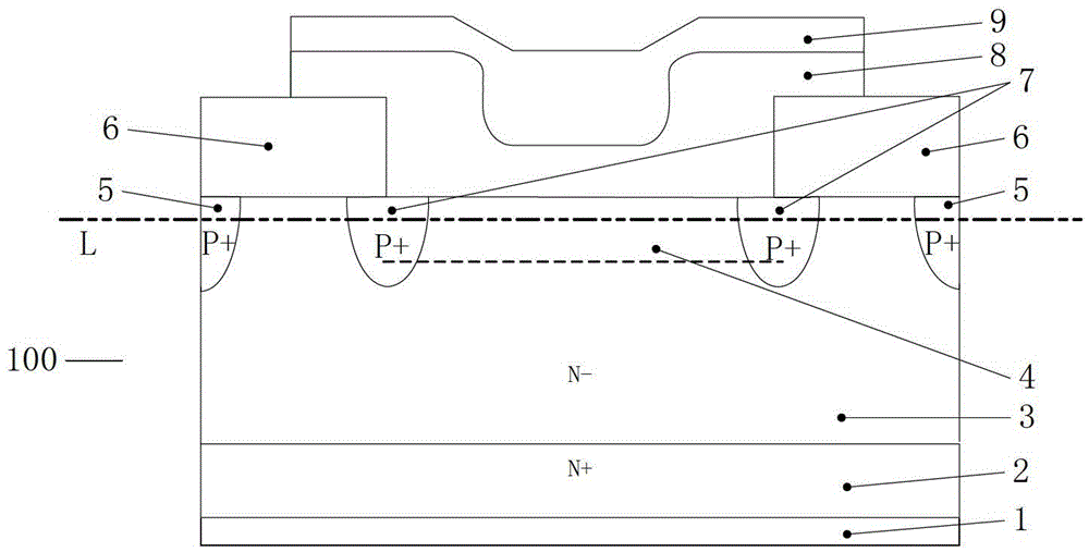
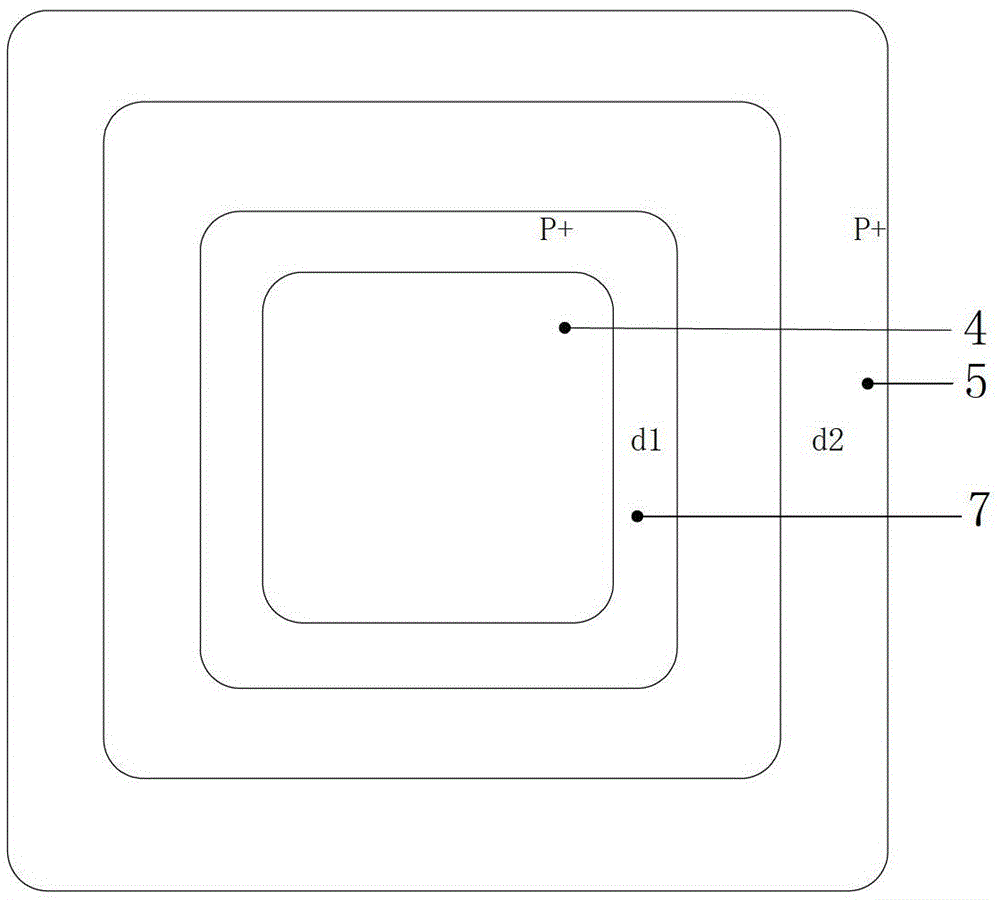
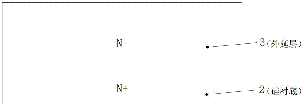
[0054] Using the above manufacturing method, a Schottky diode with a reverse breakdown voltage of 30V was fabricated. In the Schottky diode, the width d1 of the P+ inner ring is about 18 μm, and the width d2 of the P+ outer ring is about 40 μm. The dose of boron ion implantation is about 1×10 14 cm -2 , the depths of the inner and outer rings of P+ are about 2 μm respectively, and the design target parameters are reverse breakdown voltage V R ≥30V, V R I = 20V R ≤45μA.


PUM


Abstract

The invention relates to a Schottky diode and a manufacturing method of the Schottky diode. The Schottky diode comprises a cathode metal layer, an N type silicon chip on the cathode metal layer, an insulating layer with an opening on the N type silicon chip, and an anode metal layer located in the opening and on the insulating layer. The Schottky diode further comprises a metal silicide layer located below the anode metal layer in the N type silicon chip, a high concentration P type doped inner ring located in the N type silicon chip around the metal silicide layer and a high concentration P type doped outer ring outside the high concentration P type doped inner ring. The anode metal layer consists of titanium aluminum metal. According to the Schottky diode prepared by the invention, not only is the performance parameter improved, but also the yield of the Schottky diodes is remarkably improved without adding process steps.

Description

technical field [0001] The present invention relates to Schottky devices. More specifically, the present invention relates to a Schottky diode and a method of manufacturing the same. Background technique [0002] At present, in the production process of Schottky diode chips, a three-layer metal of Ti-Ni-Ag and an N-epitaxial layer are generally used to form a Schottky barrier structure. There are currently two disadvantages in this structure. First, the process precision of titanium-nickel-silver wet etching is very high, and the stability of this key process often restricts the characteristic parameters of Schottky diodes. A little carelessness in the wet etching process can easily cause low reverse breakdown voltage and large leakage current of the Schottky diode, thus affecting the performance of the Schottky diode and the yield of the chip. Secondly, chips produced by the titanium-nickel-silver process are susceptible to surface oxidation due to the influence of ambien...

Claims


Application Information

Patent Timeline
Patent Type & Authority Patents(China)
IPC IPC(8): H01L29/872H01L29/06H01L29/47H01L21/329H01L21/28
Inventor 王剑敏
Owner BEIJING YANDONG MICROELECTRONICS
Why Eureka
Try Eureka