Method for preparing electromagnetic energy harvester using micro-nano processing technology

An energy harvester and micro-nano processing technology, applied in the direction of microstructure technology, technology for producing decorative surface effects, decorative art, etc., can solve the problems of unfavorable large-scale production and processing, low efficiency, limited output voltage, etc.

Active Publication Date: 2016-02-17
PEKING UNIV
View PDF6 Cites 0 Cited by
  • Summary
  • Abstract
  • Description
  • Claims
  • Application Information

AI Technical Summary

Problems solved by technology

However, since the processing of its permanent magnets is manually pasted, it is not completely integrated processing, so it is not conducive to large-scale production and processing
At the same time, because the coil of the electromagnetic energy harvester is not efficient in cutting the magnetic induction line, its output voltage is limited
[0004] From the above introduction, it can be seen that electromagnetic energy harvesting, as a vibration energy harvesting method with obvious advantages, has no good integrated processing and preparation technology, and the output voltage also restricts its application.

Method used


Image

  • Method for preparing electromagnetic energy harvester using micro-nano processing technology
  • Method for preparing electromagnetic energy harvester using micro-nano processing technology
  • Method for preparing electromagnetic energy harvester using micro-nano processing technology

Examples


Embodiment 1

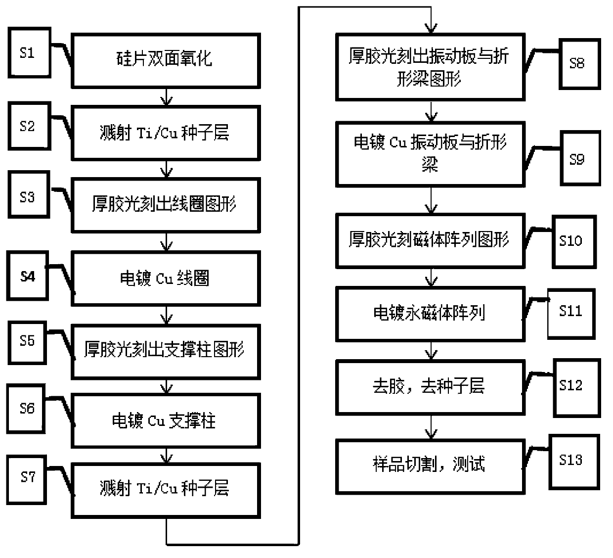
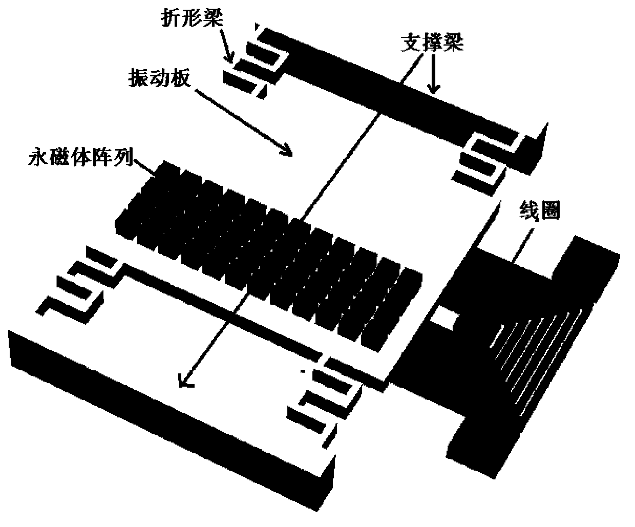
[0053] refer to figure 1 , figure 1 For the step flowchart of the energy harvester that the present invention adopts, comprise the steps:

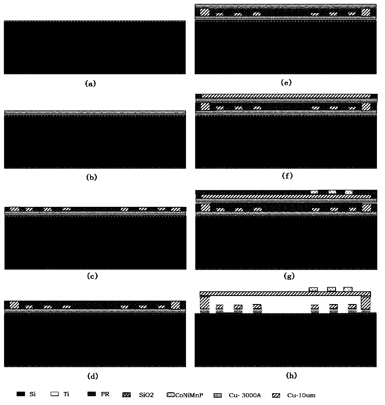
[0054] Step S1, using double-sided oxidation on a clean (100) crystalline silicon wafer silicon oxide

[0055] Step S2, sputtering metal on a clean (100) silicon wafer by sputtering Metal

[0056] Step S3, drop the photoresist on the surface of the silicon wafer, first pre-level the glue at a speed of 540r / s for 60s, and then perform the formal coating of 1500r / s for 180s to ensure that the photoresist is evenly spread on the surface of the silicon wafer. Dry the film at 100°C for 300s. Expose for 125s under the photolithography machine, then take it out. Then develop and soak in the developer for 30s. Ensure visualization under a microscope. The film was baked at 100°C for 600s.

[0057] Step S4, setting up the electroplating device, adjusting the electroplating current so that the current density is 1ASD, connecting the sili...

Embodiment 2

[0068] refer to figure 1 , figure 1 For the step flowchart of the energy harvester that the present invention adopts, comprise the steps:

[0069] Step S1, using double-sided oxidation on a clean (100) crystalline silicon wafer silicon oxide

[0070] Step S2, sputtering metal on a clean (100) silicon wafer by sputtering Metal

[0071] Step S3, drop the photoresist on the surface of the silicon wafer, first pre-level the glue at a speed of 540r / s for 60s, and then perform the formal coating of 1500r / s for 180s to ensure that the photoresist is evenly spread on the surface of the silicon wafer. Dry the film at 100°C for 300s. Expose for 125s under the photolithography machine, then take it out. Then develop and soak in the developer for 30s. Ensure visualization under a microscope. The film was baked at 100°C for 600s.

[0072] Step S4, setting up the electroplating device, adjusting the electroplating current so that the current density is 1ASD, connecting the sili...

Embodiment 3

[0083] refer to figure 1 , figure 1 For the step flowchart of the energy harvester that the present invention adopts, comprise the steps:

[0084] Step S1, using double-sided oxidation on a clean (100) crystalline silicon wafer silicon oxide

[0085] Step S2, sputtering metal on a clean (100) silicon wafer by sputtering Metal

[0086] Step S3, drop the photoresist on the surface of the silicon wafer, first pre-level the glue at a speed of 540r / s for 60s, and then perform the formal coating of 1500r / s for 180s to ensure that the photoresist is evenly spread on the surface of the silicon wafer. Dry the film at 100°C for 300s. Expose for 125s under the photolithography machine, then take it out. Then develop and soak in the developer for 30s. Ensure visualization under a microscope. The film was baked at 100°C for 600s.

[0087] Step S4, setting up the electroplating device, adjusting the electroplating current so that the current density is 1ASD, connecting the sili...


PUM

PropertyMeasurementUnit
thicknessaaaaaaaaaa
thicknessaaaaaaaaaa

Abstract

The invention relates to the production field of micromechanical systems, in particular to the technical field of micro-nanometer machining, and more in particular to a production method for a vibration energy collector capable of being integrally processed. The method comprises the steps of optional selection of processing substrates, electroplating of Cu coils, electroplating of Cu support poles, electroplating of Cu vibration plates and foldable beams, electroplating of permanent magnet arrays, degumming, and removing seed layers to obtain the electromagnetic energy collector through cutting. The energy collector can improve output voltage through serial connection of coils. The requirements of overall integration processing can be metthrough the preparation of permanent magnet CoNiMnP alloys. And at the same time, the novel structural design largely improves the output voltage of the energy collector, and largely improves the energy collecting efficiency. Meanwhile, the optimization of the energy collector can be achieved through changing geometric sizes and arrangement positions of the permanent magnet arrays. And the change of the output voltage and resonant frequency can be achieved through changing the thicknesses and the lengths of the vibration plates and the foldable beams.

Description

technical field [0001] The invention relates to the field of micro-mechanical system manufacturing, in particular to the field of micro-nano processing technology, and in particular to a method for preparing an electromagnetic energy harvester using micro-nano processing technology. Background technique [0002] Micro-Electro-Mechanical System (MEMS) is a new type of interdisciplinary technology, which involves many disciplines such as mechanics, electronics, chemistry, physics, optics, biology, and materials. Components prepared using micro-nano processing technology have a wide range of applications and prospects. The invention relates to a device capable of collecting vibration energy in the surrounding environment and storing it as electrical energy. It can effectively collect and store low-frequency vibrations that are ubiquitous in the environment. Mechanical vibration is the most common form of energy, so converting vibration energy into electrical energy is the foc...

Claims


Application Information

Patent Timeline
Patent Type & Authority Patents(China)
IPC IPC(8): B81C1/00H02K35/02C25D3/56
Inventor 张海霞李忠亮韩梦迪
Owner PEKING UNIV
Why Eureka
Try Eureka