
LED substrate removal method and LED chip prepared thereby

A technology of LED chips and substrates, applied in electrical components, circuits, semiconductor devices, etc., can solve the problems of difficult to meet demand for finished product quality, limited luminous efficiency, harshness, etc., and achieve the effect of reducing cost input

Inactive Publication Date: 2013-03-13
沈李豪
View PDF10 Cites 5 Cited by
  • Summary
  • Abstract
  • Description
  • Claims
  • Application Information

AI Technical Summary

Problems solved by technology

But for LED chips, the substrate has two sides. During the growth process of each layer of the chip, the LED chip must need the substrate. However, after the production is completed, the substrate becomes the weakness of the finished product. Existence, the LED light-emitting surface is at most 5 sides, and the luminous efficiency is therefore limited in its essential structure
In the prior art, there are many ways to use machine grinding, but because the hardness of sapphire is very high, the hardness of natural substances is second only to diamond, so the materials required for grinding are also harsh, otherwise the use of poor quality grinding tools will reduce the wear degree. It will be very large, and the quality of the finished product obtained after grinding is difficult to meet the demand

Method used


Image

  • LED substrate removal method and LED chip prepared thereby

Examples


Embodiment Construction

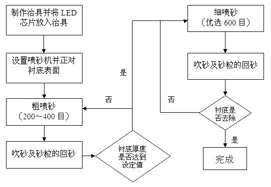
[0018] The present invention will be described in further detail below in conjunction with the accompanying drawings. figure 1 A kind of embodiment that it adopts is represented schematically.

[0019] A method for removing an LED substrate according to the present invention comprises the following steps:

[0020] S1. Make a jig and put the LED chip into the fixed position of the jig;

[0021] S2. Set up the sandblasting machine, and move the nozzle of the sandblasting machine to face the surface of the LED substrate that needs to be removed;

[0022] S3. Select sand with a mesh number of 200-400 for rough sandblasting;

[0023] S4. Perform sand blowing and sand return on the surface of the LED substrate after rough sand blasting;

[0024] S5. Select sand with a mesh number of 500-650 for fine sandblasting;

[0025] S6. Carry out sand blasting and sand return of sand grains on the surface of the LED substrate after fine sand blasting;

[0026] S7. Determine whether the LE...


PUM


Abstract

The invention relates to removal processing methods of LED substrates, especially to an LED substrate removal method and an LED chip prepared thereby. The method comprises the steps of: making a jig and placing an LED chip into a jig fixation position; setting a sand blasting machine, moving the nozzle of the sand blasting machine to make the nozzle in a position over against an LED substrate surface needing substrate removal; selecting sand with a size of 200-400 meshes to conduct coarse sand blasting; subjecting the LED substrate surface undergoing coarse sand blasting to sand blowing and sand recovery; electing sand with a size of 500-650 meshes to perform fine sand blasting; subjecting the LED substrate surface undergoing fine sand blasting to sand blowing and sand recovery; and judging whether the LED substrate is removed. In the invention, the sand blasting technological mode is used to thin and remove the LED substrate and conduct surface roughening on the LED substrate simultaneously. A twice sand blasting pattern is utilized. For the first time, coarse sand blasting is employed to substantially thin the primarily thick substrate. During removal, a residual-free surface needs to be guaranteed at last, so that finer sand needs to be adopted then. Also, compared with existing grinding tools, the use cost is much lower, and the input cost is substantially reduced.

Description

technical field [0001] The invention relates to an LED substrate, in particular to a method for removing an LED substrate and an LED structure obtained therefrom. Background technique [0002] For the production of LED chips, the primary consideration in the selection of existing LED chip substrates is what kind of suitable substrate should be used. Each substrate needs to be used for different equipment and LED requirements. The existing three The widely used LED substrate materials are sapphire, silicon and silicon carbide. The thermal conductivity of silicon carbide is much higher than that of sapphire, but due to existing technical obstacles, its manufacturing cost is relatively high, and it is still a long way to go before it can be fully commercialized and widely used. The production technology of sapphire substrate is mature, and its stability is also high. The device made by it has good quality, high mechanical strength, and is easier to handle and clean, so it is w...

Claims


Application Information

Patent Timeline
IPC IPC(8): B24C1/08H01L33/00
Inventor 沈李豪
Owner 沈李豪
Learn More