Method for eliminating bridging in contact hole technique

A contact hole and process technology, applied in metal material coating process, coating, gaseous chemical plating, etc., can solve problems such as circuit failure, achieve good adhesion, eliminate bridging phenomenon, and avoid the generation of defective particles Effect

Active Publication Date: 2013-01-30
INST OF MICROELECTRONICS CHINESE ACAD OF SCI
View PDF3 Cites 4 Cited by
  • Summary
  • Abstract
  • Description
  • Claims
  • Application Information

AI Technical Summary

Problems solved by technology

Due to the storage of the bridge part 18, a plurality of contact plugs 17 are bridged and short-circuited, causing a circuit failure

Method used


Image

  • Method for eliminating bridging in contact hole technique
  • Method for eliminating bridging in contact hole technique
  • Method for eliminating bridging in contact hole technique

Examples


Embodiment Construction

[0018] Hereinafter, the present invention is described by means of specific embodiments shown in the drawings. It should be understood, however, that these descriptions are exemplary only and are not intended to limit the scope of the present invention. Also, in the following description, descriptions of well-known structures and techniques are omitted to avoid unnecessarily obscuring the concept of the present invention.

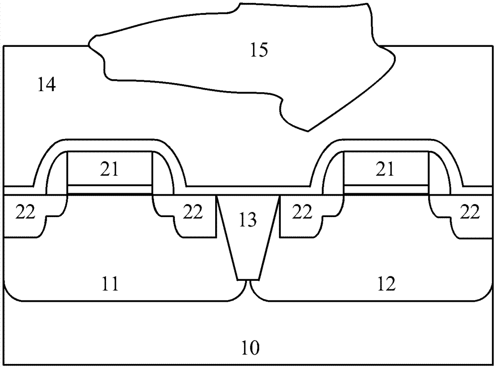
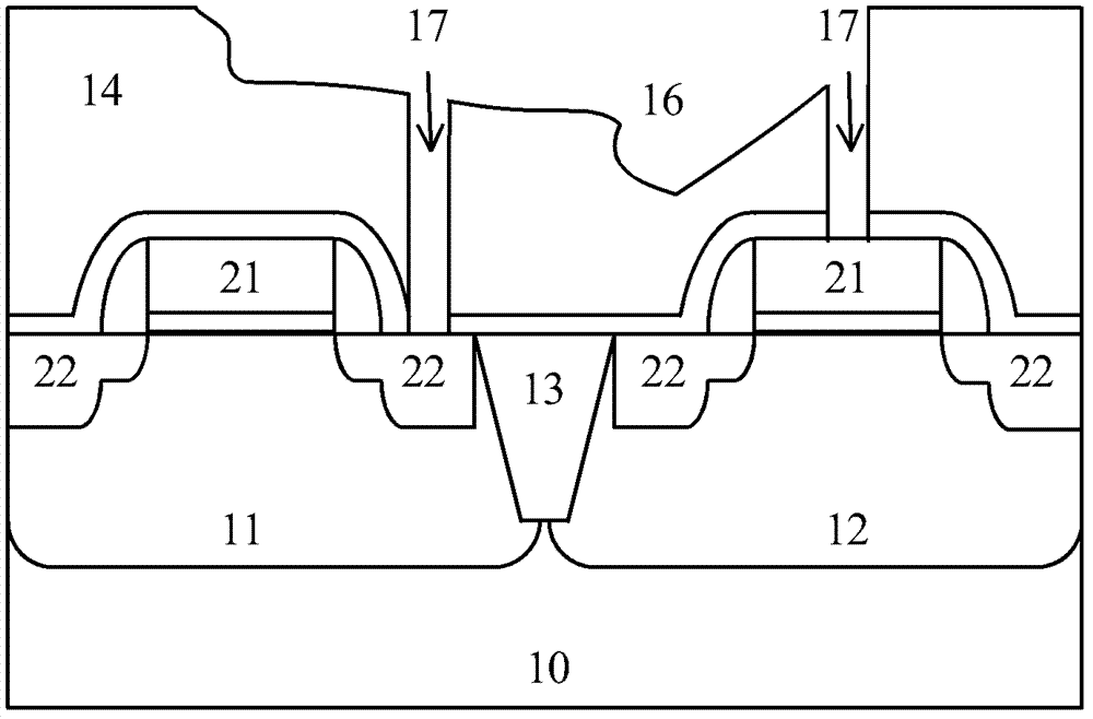
[0019] Embodiments of the present invention relate to a dry cleaning process after dielectric film deposition using a high-density plasma chemical vapor deposition (HDP CVD) method, so as to achieve perfect particle requirements on the deposited wafer surface, thereby improving the performance of the HDP CVD process. Technical yield, eliminating the bridging phenomenon in the contact hole process.

[0020] According to the present invention, see attached Figure 9 First, a semiconductor substrate 10 is provided, on which an N well 11 and a P well 12 are p...


PUM


Abstract

The invention relates to a method for eliminating bridging in a contact hole technique, which provides a cleaning menu comprising a plurality of adaptive protective film deposition technical steps. A laminated adaptive protective film is formed on the side wall of the chamber of HDP CVD (high-density plasma chemical vapor deposition) equipment; and the laminated adaptive protective film with favorable adhesiveness, compactness and uniformity can protect the side wall of the chamber of the HDP CVD equipment from damage of plasma, avoids the generation of defective granules, enhances the yield of the HDP CVD technique, and eliminates the phenomenon of bridging in the contact hole technique.

Description

technical field [0001] The invention relates to the field of semiconductor integrated circuit manufacturing, in particular to a method for eliminating contact bridges in a contact hole process. Background technique [0002] Semiconductor integrated circuits are moving forward with the schedule predicted by Moore's Law, the feature size of the device is developing towards a small-scale structure, and the integration level is continuously improving. With the continuous miniaturization of feature size, the integration level of a single chip has reached as high as 10 8 ~10 9 , and at the same time, the requirements for the production process are getting higher and higher, therefore, it becomes very critical to reduce the size and density of defects in the manufacturing process. A 1-micron dust on a transistor with a size of 100 microns may not be a problem, but for a 1-micron transistor, it will be a fatal defect that causes device failure, so it is especially proposed for che...

Claims


Application Information

Patent Timeline
Patent Type & Authority Applications(China)
IPC IPC(8): H01L21/205H01L21/762
CPCH01L21/762C23C16/4404C23C16/308C23C16/345H01L21/02C23C16/402C23C16/56C23C16/50H01L21/76837C23C16/505H01L21/205
Inventor 王桂磊李俊峰赵超
Owner INST OF MICROELECTRONICS CHINESE ACAD OF SCI
Why Eureka
Try Eureka