
A method for manufacturing a base material having gold-coated metallic fine pattern, a base material having gold-coated metallic fine pattern, a printed wiring board, an interposer and a semiconductor device

A printed wiring board and micro-pattern technology, applied in semiconductor devices, metal material coating processes, semiconductor/solid-state device components, etc., can solve problems such as the inability to fully prevent abnormal metal precipitation, and achieve excellent peel strength and prevent abnormality. Excellent effect of precipitation and adhesion

Inactive Publication Date: 2013-01-23
SUMITOMO BAKELITE CO LTD
View PDF8 Cites 21 Cited by
  • Summary
  • Abstract
  • Description
  • Claims
  • Application Information

AI Technical Summary

Problems solved by technology

[0022] However, even with the method using a specific removing liquid disclosed in Patent Document 2 and the method using a combination of the above specific removing liquid and a known bridging preventing liquid, it is possible to perform electroless nickel-gold plating on the surface of a circuit formed by the SAP method. During electroless metal plating of electroless plating treatment or electroless nickel-palladium-gold plating treatment, the abnormal deposition of metal around the circuit cannot be sufficiently prevented

Method used


Image

  • A method for manufacturing a base material having gold-coated metallic fine pattern, a base material having gold-coated metallic fine pattern, a printed wiring board, an interposer and a semiconductor device
  • A method for manufacturing a base material having gold-coated metallic fine pattern, a base material having gold-coated metallic fine pattern, a printed wiring board, an interposer and a semiconductor device
  • A method for manufacturing a base material having gold-coated metallic fine pattern, a base material having gold-coated metallic fine pattern, a printed wiring board, an interposer and a semiconductor device

Examples


Embodiment 1

[0279] (Example 1: (a) Treatment, ENEPIG process)

[0280] 1. Preparation of Primer Resin

[0281]In a mixed solvent of dimethylacetamide and methyl ethyl ketone, 31.5 parts by weight of a methoxynaphthalene aralkyl type epoxy resin (manufactured by DIC Corporation, EPICLON HP-5000) as an epoxy resin, as a cyanide 26.7 parts by weight of a novolak-type cyanate ester resin (Primaset PT-30, manufactured by LONZA), 31.5 parts by weight of a polyamide resin (KAYAFLEX BPAM01, manufactured by Nippon Kayaku Co., Ltd.), and imidazole ( Shikoku Chemicals Co., Ltd., CUREZOL 1B2PZ) 0.3 parts by weight, stirred for 30 minutes, and dissolved. Furthermore, 0.2 parts by weight of an epoxysilane coupling agent (manufactured by Unicar Japan, A187) as a coupling agent and spherical fused silica as an inorganic filler (manufactured by Fuso Chemical Industry Co., Ltd., SP-7, average particle diameter 0.75 μm) and 9.8 parts by weight were stirred for 10 minutes using a high-speed stirring device...

Embodiment 2

[0317] (Example 2: (b) treatment, ENEPIG process)

[0318] In the surface treatment process of embodiment 1, do not carry out the surface treatment that uses the liquid medicine that contains nitric acid and chloride ion, after the test piece is immersed in the solution containing KCN of concentration 20g / liter, liquid temperature 25 ℃ for 1 minute, carry out 3 Second water wash (treatment with KCN).

Embodiment 3

[0319] (Example 3: (c) treatment, ENEPIG process)

[0320] In the surface treatment process of Example 1, the surface treatment using a chemical solution containing nitric acid and chloride ions was not performed, and the desmearing treatment using a chemical solution (surface treatment using a solution containing sodium permanganate) was performed as follows.

[0321] (1) Resin surface swelling treatment

[0322] The test piece was immersed in a mixed solution (pH 12) of a commercially available sodium hydroxide solution containing an ethylene glycol-based solvent (Securiganth P preparation solution manufactured by ATOTECH Corporation) at a liquid temperature of 60°C for 2 minutes, and then washed three times with water.

[0323] (2) Resin surface roughening treatment

[0324] After immersing the test piece in a roughening treatment solution containing sodium permanganate (concentrate compact CP preparation solution manufactured by ATOTECH Co., Ltd.) at a liquid temperature ...


PUM

PropertyMeasurementUnit
surface roughnessaaaaaaaaaa
widthaaaaaaaaaa
surface roughnessaaaaaaaaaa

Abstract

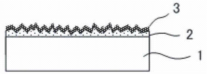
A method for manufacturing a base material having gold-coated metallic fine pattern, comprising the steps of: preparing a base material having a supporting surface composed of resin; forming a primer resin layer with surface roughness of 0.5 [mu] m or less on the supporting surface, and forming metallic fine pattern on the primer resin layer by SAP method to obtain a base material having a metallic fine pattern; gold-coating at least part of the surface of the metallic fine pattern; wherein palladium is removed from the base material having the metallic fine pattern at any time before the gold-coating step.

Description

technical field [0001] The present invention relates to a method of manufacturing a base material with a fine pattern of gold-plated metal, a base material with a fine pattern of gold-plated metal manufactured by the method, and particularly relates to printed wiring boards such as motherboards and interposers And a semiconductor device using the above-mentioned printed wiring board. Background technique [0002] In recent years, high-density integration and high-density mounting of electronic components have been progressing along with demands for higher functionality, weight reduction, miniaturization, and thinning of electronic equipment. The circuit wiring of these printed wiring boards used in electronic equipment tends to be denser and more complicated, and the miniaturization of circuit patterns has been progressing. [0003] In particular, miniaturization of circuit patterns is required on the semiconductor element mounting surface of a printed wiring board called a...

Claims


Application Information

Patent Timeline
Patent Type & Authority Applications(China)
IPC IPC(8): H05K3/18H01L23/12H05K3/22
CPCH01L23/49827H05K3/244C23C18/2086H01L2924/15311C23C18/22H01L23/49816C23C18/44H05K3/108C23C18/1689H01L2224/32225C23C18/2006H05K3/387C23C18/34C23C18/00H01L2224/73204H01L24/48C23C18/30C23C18/1651H01L2224/48227C23C18/36H05K2201/0761C23C18/1653C25D5/022C23C18/1844H01L2224/16227H01L2224/45144H01L2224/16225H01L2224/73265H01L2224/48091H01L2224/48228H01L2224/48465H01L2924/15174H01L2924/00014H01L24/45H01L24/73H01L2924/181H01L2224/05571H01L2224/05573H01L24/16H01L2224/131H01L2924/00012H01L2924/00H01L2224/05599H01L2924/014H05K3/18H01L23/12H05K3/22
Inventor 橘贤也伊藤哲平三井保明
Owner SUMITOMO BAKELITE CO LTD
Learn More