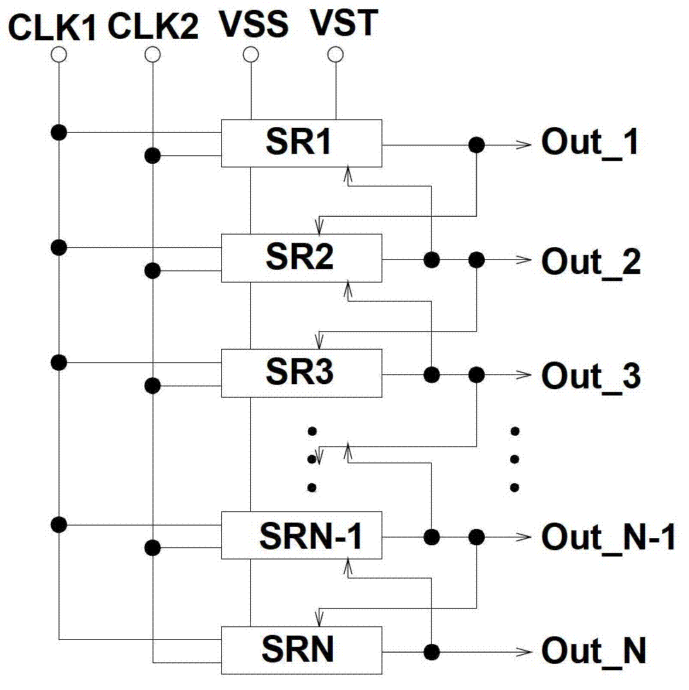
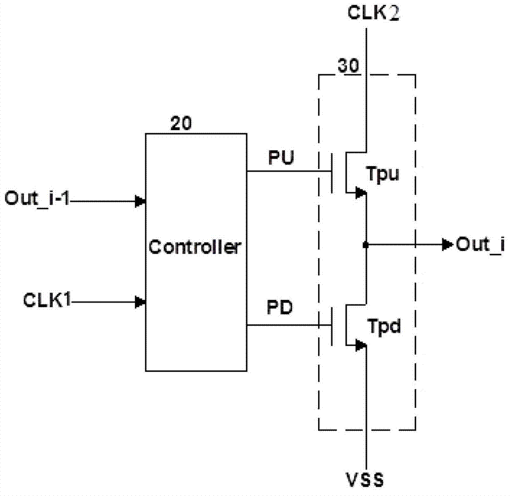
Shifting register, a grid driver and a display device
A shift register and gate technology, which is applied in the field of gate drivers, display devices, and shift registers, can solve problems such as changes in threshold voltage, damage to the stability of shift registers, and wrong outputs, and achieve the effect of improving stability
- Summary
- Abstract
- Description
- Claims
- Application Information
AI Technical Summary
Problems solved by technology
Method used
Image
Examples
Embodiment 1
[0053] Such as Figure 4 Shown, in the shift register of the present embodiment:
[0054] The pull-up module includes: a first TFT T2 and a capacitor Cb, the gate of the TFT T2 is connected to the pull-up node PU, the drain is connected to the first clock signal input terminal CLK1, and the source is connected to the output terminal Out_i; the capacitor Cb is connected to the TFT T2 between the gate and source.
[0055] The pull-down module includes: a second TFT T6_P and a third TFT T6_N. The gate of TFT T6_P is connected to the first pull-down node PD_P, the drain is connected to the signal output terminal Out_i, and the source is connected to the low-level DC signal input terminal VSS; the gate of the third TFT T6_N is connected to the second pull-down node PD_N , the drain is connected to the signal output terminal Out_i, and the source is connected to the low-level DC signal input terminal VSS. When one of the pull-down nodes PD_P and PD_N is at a high level, TFT T6_P a...
Embodiment 2
[0075] Such as Figure 6 As shown, compared with the shift register of Embodiment 1, the shift register of this embodiment has removed the TFTs T7_P, T7_N and corresponding connecting wires. Its working sequence diagram and Figure 5 gives exactly the same, but relative to Figure 4 , the reduction of TFT T7_P, T7_N will be reduced in Figure 5 The degree of discharge to the nodes PD_P and PD_N at the beginning of the t0 time period shown in , the discharge to the nodes PD_P and PD_N in the t0 time period is completed by TFT T8_P and T8_N.
Embodiment 3
[0077] Such as Figure 7 As shown, compared with the shift register of Embodiment 1, the shift register of this embodiment has the sixteenth TFT T10_P added to the first pull-down control unit, and the seventeenth TFT T10_N and corresponding connections have been added to the second pull-down control unit Wire. Figure 8 The timing diagram of its work is given, and Figure 5 Compared to when the change occurs in time period t0, the level of PD_P is determined by Figure 5 given the high level becomes Figure 8 The low level shown, the other time periods are the same. This is due to the Figure 7 In , the gates of TFT T10_P and T10_N are connected to Out_i+1 terminal, in Figure 8 In the time period t2 shown, Out_i+1 is at a high level, so the TFTs T10_P and T10_N connected to the gate are both turned on, and the nodes PD_P and PD_N are connected to the low-level line VSS, so that the nodes PD_P and PD_N are both low level, even though CLK2 is at a high level at this time...
PUM
 Abstract
Description
Claims
Application Information
 - Generate Ideas
- Intellectual Property
- Life Sciences
- Materials
- Tech Scout
- Unparalleled Data Quality
- Higher Quality Content
- 60% Fewer Hallucinations
Browse by: Latest US Patents, China's latest patents, Technical Efficacy Thesaurus, Application Domain, Technology Topic, Popular Technical Reports.
© 2025 PatSnap. All rights reserved.Legal|Privacy policy|Modern Slavery Act Transparency Statement|Sitemap|About US| Contact US: help@patsnap.com


