Micromechanical filter with fully sealed structure
A filter and micro-mechanical technology, which is applied in the field of micro-mechanical filters with a fully sealed structure, can solve the problems of being unable to achieve full sealing and reduce the volume of the filter, and achieve the goals of reducing volume, improving packaging efficiency, and reducing packaging volume Effect
- Summary
- Abstract
- Description
- Claims
- Application Information
AI Technical Summary
Problems solved by technology
Method used
Image
Examples
Embodiment 1
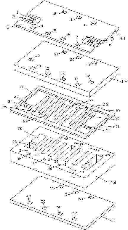
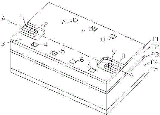
[0032] The micromechanical filter with a fully sealed structure provided by the present invention, the filter includes an upper dielectric layer and a lower dielectric layer stacked up and down, interdigitated electrodes with tapped signal lines are arranged between the upper dielectric layer and the lower dielectric layer The middle metal electrode layer; the upper surface of the lower dielectric layer in contact with the middle metal electrode layer is provided with a first cavity matching the interdigitated electrode tap signal line; the lower dielectric layer in contact with the middle metal electrode layer A second cavity matching the interdigitated electrode fingers is provided on the surface; a metal layer on the upper surface of the upper dielectric layer is arranged above the surface of the upper dielectric layer, and a metal layer on the lower surface of the lower dielectric layer is arranged below the surface of the lower dielectric layer. The upper and lower dielect...
Embodiment 2
[0037] The fully sealed micromechanical filter will be further described as follows:
[0038] figure 1 It is a layered perspective diagram of a micro-mechanical filter with a fully-sealed structure. The micro-mechanical filter with a fully-sealed structure based on micro-mechanical technology is composed of two dielectric layers superimposed on top of each other. There is a micro-mechanical process between the two dielectric layers. The metal electrode layer made; wherein, f1 is the metal layer on the upper surface of the upper dielectric layer, f2 is the upper dielectric layer, f3 is the middle metal layer, f4 is the lower dielectric layer, f5 is the lower surface metal layer of the lower dielectric layer, and the upper dielectric layer is There are cavities prepared by etching process on the surface; there are through holes on the upper and lower dielectric layers, and a metal layer is prepared on the inner wall of the through holes; there are surface electrode layers made b...
PUM
| Property | Measurement | Unit |
|---|---|---|
| thickness | aaaaa | aaaaa |
| thickness | aaaaa | aaaaa |
| thickness | aaaaa | aaaaa |
Abstract
Description
Claims
Application Information
 - R&D Engineer
- R&D Manager
- IP Professional
- Industry Leading Data Capabilities
- Powerful AI technology
- Patent DNA Extraction
Browse by: Latest US Patents, China's latest patents, Technical Efficacy Thesaurus, Application Domain, Technology Topic, Popular Technical Reports.
© 2024 PatSnap. All rights reserved.Legal|Privacy policy|Modern Slavery Act Transparency Statement|Sitemap|About US| Contact US: help@patsnap.com


