High accuracy beam placement for local area navigation

A particle beam and sample technology, applied in the direction of discharge tubes, semiconductor devices, semiconductor/solid-state device testing/measurement, etc.

Active Publication Date: 2012-12-12
FEI CO
View PDF10 Cites 6 Cited by
  • Summary
  • Abstract
  • Description
  • Claims
  • Application Information

AI Technical Summary

Problems solved by technology

Such a high-resolution scan (64K) of a 100µm x 100µm a...

Method used


Image

  • High accuracy beam placement for local area navigation
  • High accuracy beam placement for local area navigation
  • High accuracy beam placement for local area navigation

Examples


Embodiment Construction

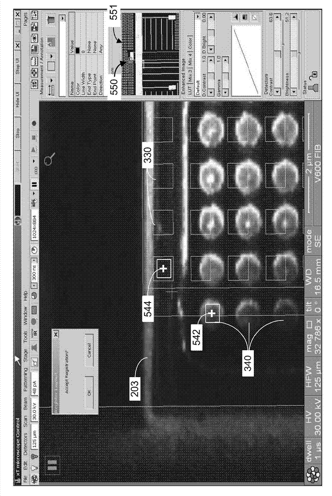
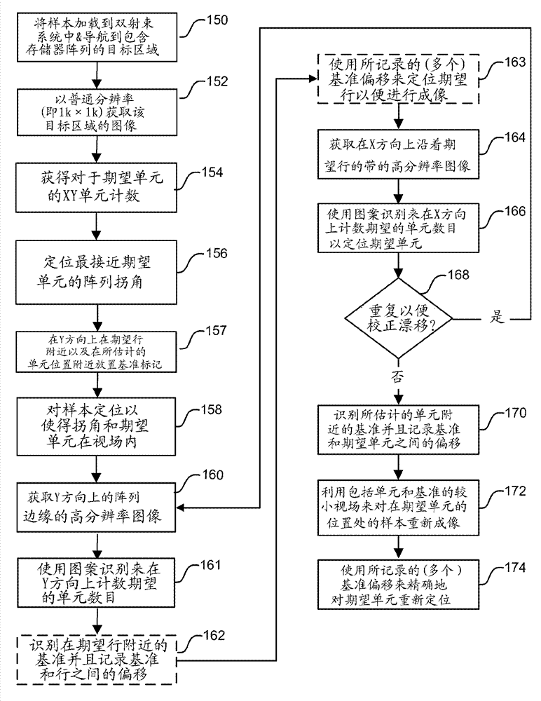
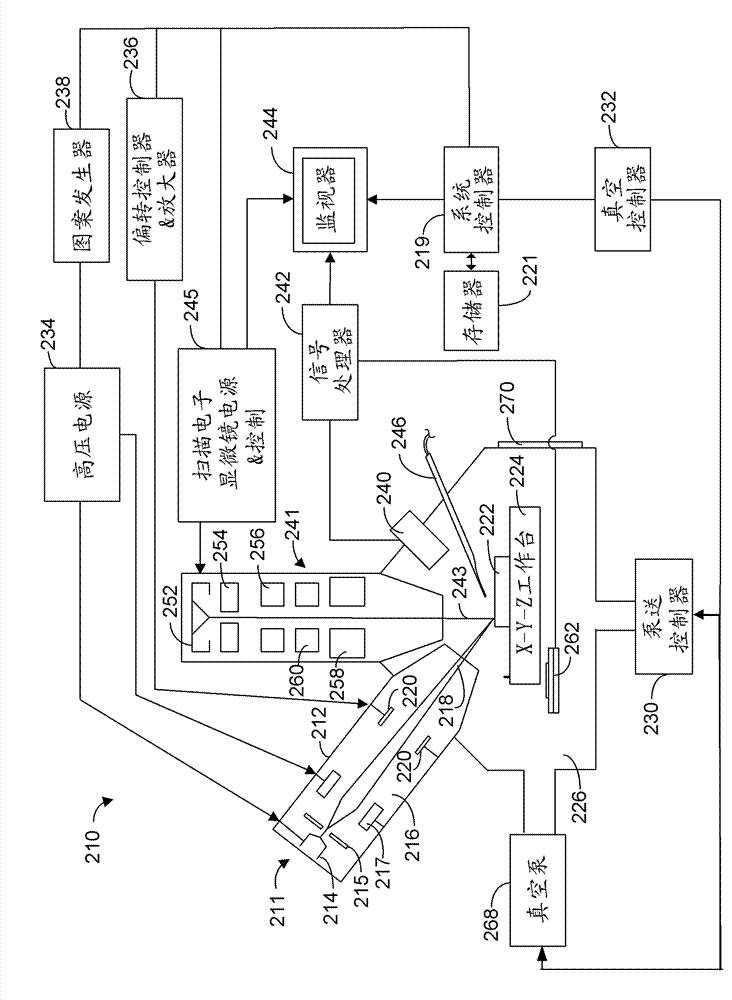
[0032] A preferred embodiment of the invention is directed to a method for high precision beam placement for local area navigation in the field of semiconductor chip manufacturing. The present invention exemplifies such a situation where it is possible to achieve a site of interest within a relatively large localized area (e.g., an area of ​​200 μm x 200 μm) even when the stage / navigation system is not normally capable of high-accuracy navigation. A method for high-precision navigation.

[0033]According to a preferred embodiment of the present invention, a high resolution image of a relatively large target area (a large area including the location of one or more appropriate alignment marks and features of interest) is first acquired. For example, a suitably high resolution region might be 250 μm wide, with a resolution of about 4096 pixels wide. According to a preferred embodiment, CAD polygons are used to cover the region of interest and two or three point CAD polygon re-re...


PUM


Abstract

The invention relates to high accuracy beam placement for local area navigation. An improved method of high accuracy beam placement for local area navigation in the field of semiconductor chip manufacturing is described. Preferred embodiments of the present invention can be used to rapidly navigate to one single bit cell in a memory array or similar structure, for example to characterize or correct a defect in that individual bit cell. High-resolution scanning is used to scan a "strip" of cells on the one edge of the array (along either the X axis and the Y axis) to locate a row containing the desired cell followed by a similar high-speed scan along the located row (in the remaining direction) until the desired cell location is reached. This allows pattern-recognition tools to be used to automatically "count" the cells necessary to navigate to the desired cell, without the large expenditure of time required to image the entire array.

Description

technical field [0001] The present invention relates to stage navigation and beam placement in particle beam systems, and in particular to high precision to a site of interest on a sample surface using the acquisition of high resolution images by a FIB or SEM device. degree local area navigation. Background technique [0002] Semiconductor fabrication, such as integrated circuit fabrication, is often accompanied by the use of photolithography. A semiconductor substrate (typically a silicon wafer) on which circuitry is being formed is coated with a material such as photoresist that changes solubility when exposed to radiation. A lithographic tool, such as a mask or reticle, positioned between the radiation source and the semiconductor substrate casts a shadow to control which regions of the substrate will be exposed to the radiation. After exposure, the photoresist is removed from the exposed or unexposed areas, leaving a patterned photoresist layer on the wafer that protec...

Claims


Application Information

Patent Timeline
IPC IPC(8): H01L21/66
CPCH01L22/12H01J2237/31749H01J37/222G06T2207/10061G06T7/0042H01J37/3045H01J37/28G06T2207/30148H01L2924/0002G06T7/73H01L2924/00
Inventor R.L.瓦肖尔R.J.杨C.吕P.D.卡尔森
Owner FEI CO
Why Eureka
Try Eureka