


Quick Research
Generate reliable direction feasibility study reports for your R&D in just a few steps.

Technical Q&A
Discover and master advanced knowledge NOW. Basics, ideas, possibilities, all at once.

Find Solutions
As an expert in R&D theories, this can generate solutions to your technical problems instantly.

Evaluate Feasibility
Analyze your overall solution with one click, know your potential R&D risks in advance.

Monitor Landscape
Get weekly tech updates, stay abreast of the latest tech innovations and key insights.
Solar cell and method for producing grid line electrode of solar cell
A solar cell and manufacturing method technology, which is applied in the direction of circuits, electrical components, and final product manufacturing, etc., can solve the problem that the thickness and width of grid electrodes cannot be well controlled accurately, cannot be completed at one time, and the amount of waste of silver materials is large, etc. problem, to achieve the effect of improving light conversion efficiency, simple production method and high product quality
- Summary
- Abstract
- Description
- Claims
- Application Information
AI Technical Summary
Problems solved by technology
Method used
Image

Examples
Embodiment approach 1
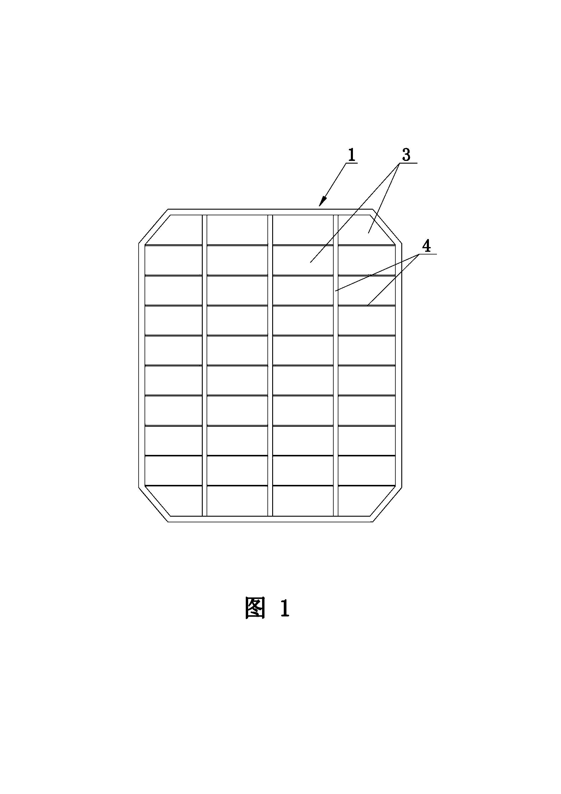
[0033] refer to figure 1 , figure 2 , the preparation method of the grid wire electrode of the solar cell comprises the following steps:
[0034] A. Die loading: press-fit a grid mold frame 2 corresponding to the required grid electrode on the surface of the battery sheet 1, and the bottom surface of the grid-shaped mold frame 2 is close to the surface of the battery sheet 1;
[0035] B. Coating: fill the cavity of the grid formwork 2 with a transparent insulating material, so that the surface of the cell 1 is uniformly coated with a transparent insulating film layer 3, and the thickness of the transparent insulating film layer 3 is 2 to 30 microns, more Specifically, the above-mentioned transparent insulating material is silica gel or an insulating polymer material, such as EVA or PE or PET;
[0036] C. Formwork removal: Remove the grid formwork 2 to form a grid line network exposed on the surface of the battery sheet 1; if the other surface of the battery sheet 1 also ne...
Embodiment approach 2
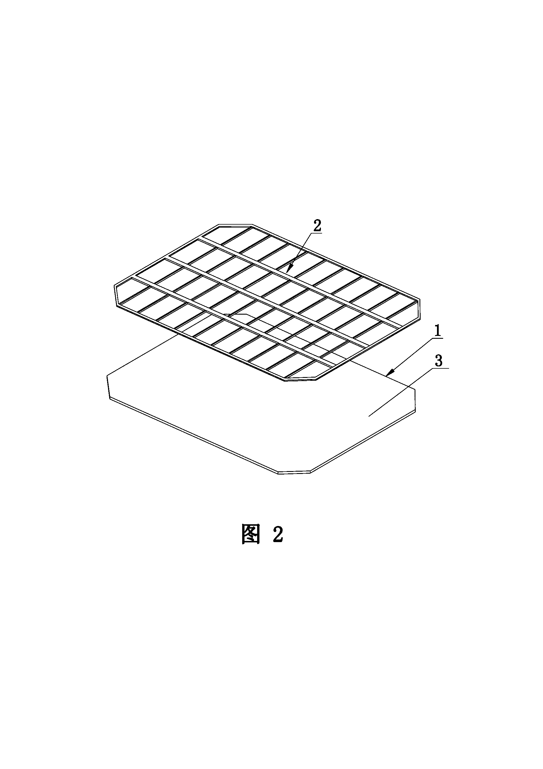
[0040] refer to figure 1 , the manufacturing method of the grid wire electrode 4 of the solar cell comprises the following steps:
[0041] A. Coating: Evenly coat a transparent insulating film layer 3 made of a transparent insulating material on the surface of the battery sheet 1. The thickness of the transparent insulating film layer 3 is 2 to 30 microns. More specifically, the above-mentioned transparent insulating material is silica gel Or insulating polymer materials, insulating polymer materials such as EVA or PE or PET;
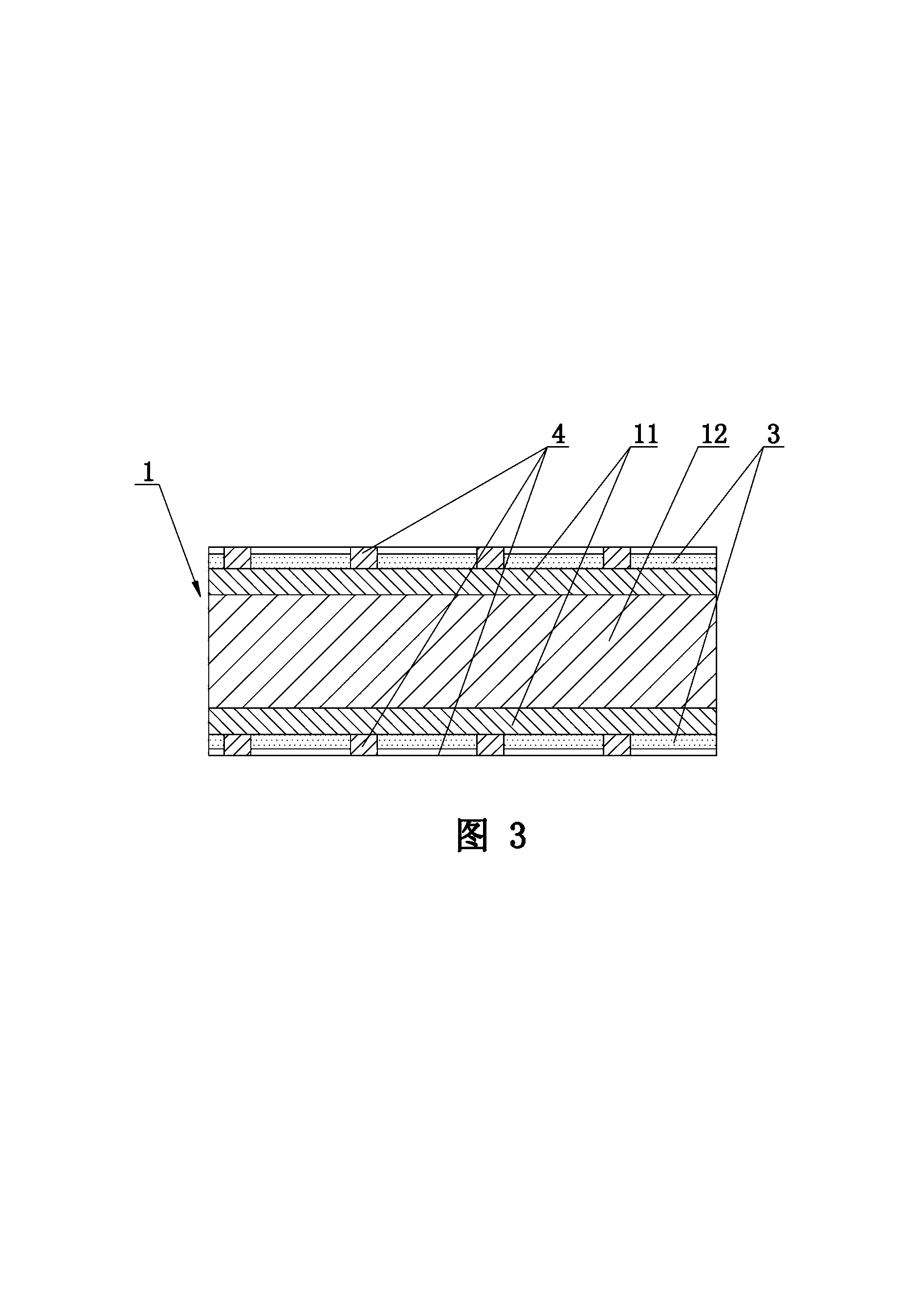
[0042] B. drying: the transparent insulating film layer 3 is dried, so that the transparent insulating film layer 3 and the battery sheet 1 are consolidated together; After B is completed and before step C begins, repeat steps A and B on the other surface of the battery sheet 1, so that both surfaces of the battery sheet 1 are coated with a transparent insulating film layer 3;
[0043] C. Delineate the network: use laser characterization or mechanica...
PUM
 Abstract
Description
Claims
Application Information
 - R&D Engineer
- R&D Manager
- IP Professional
- Industry Leading Data Capabilities
- Powerful AI technology
- Patent DNA Extraction
Browse by: Latest US Patents, China's latest patents, Technical Efficacy Thesaurus, Application Domain, Technology Topic, Popular Technical Reports.
© 2024 PatSnap. All rights reserved.Legal|Privacy policy|Modern Slavery Act Transparency Statement|Sitemap|About US| Contact US: help@patsnap.com