Semiconductor device and method of manufacturing the same
A semiconductor, conductive type technology, applied in semiconductor/solid-state device manufacturing, semiconductor devices, transistors, etc., can solve problems such as hFE being smaller than expected value, inability to obtain V-NPN transistor characteristics, etc., to achieve the effect of reasonable manufacturing process
- Summary
- Abstract
- Description
- Claims
- Application Information
AI Technical Summary
Problems solved by technology
Method used
Image

Examples
no. 1 approach 〕
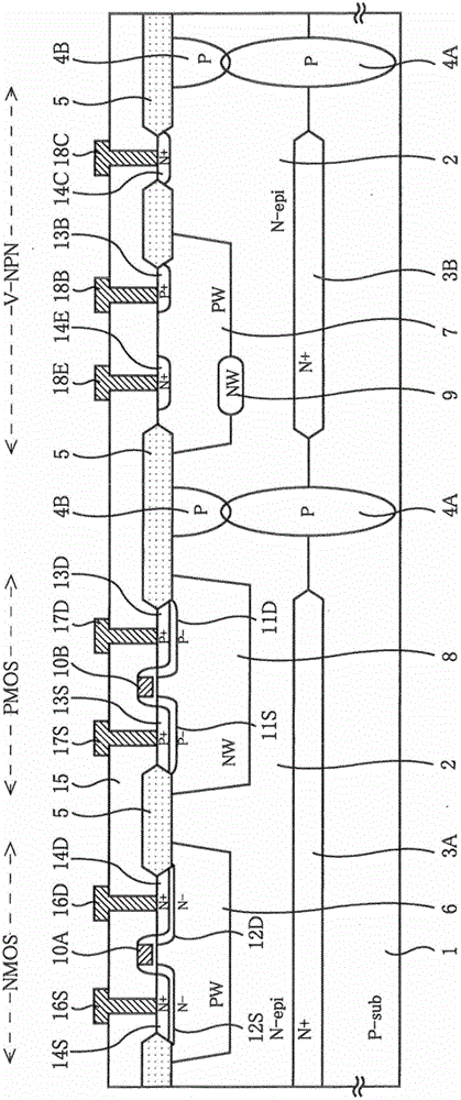
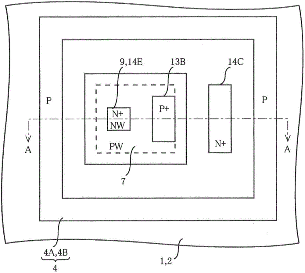
[0052] figure 1 It is a cross-sectional view of the semiconductor device according to the first embodiment of the present invention. figure 2 It is a top view of a V-NPN transistor of a semiconductor device. figure 2 The sectional view of the A-A line of figure 1 Corresponding to the cross-sectional view of the V-NPN transistor.
[0053] An N − -type epitaxial semiconductor layer 2 is formed on a semiconductor substrate 1 made of a P-type single crystal. The semiconductor substrate 1 and the N-type epitaxial semiconductor layer 2 form a PN junction. In the formation region of the NMOS transistor and the PMOS transistor, an N+ type buried layer 3A is formed across the PN junction of the semiconductor substrate 1 and the N-type epitaxial semiconductor layer 2, so as to reduce the N-type epitaxial semiconductor layer 2 (PMOS transistor) substrate) resistance.
[0054] In addition, in the formation region of the V-NPN transistor, an N+-type buried layer 3B is formed across ...
no. 2 approach 〕
[0081] Figure 4 It is a cross-sectional view of a semiconductor device according to a second embodiment of the present invention. This embodiment and the first embodiment ( figure 1 ) in that the N − -type emitter region 12E having a lower concentration than the N + -type emitter region 14E is formed in contact with the bottom of the N + -type emitter region 14E. In order to rationalize the process, the N + -type emitter region 14E is preferably formed using the process of forming the N + -type source layer 14S and the N + -type drain layer 14D of the NMOS transistor (ion implantation of N-type impurities). The N − -type emitter region 12E is preferably formed using the steps of forming the N − -type source layer 12S and the N − -type drain layer 12D of the NMOS transistor (ion implantation of N-type impurities).
[0082] The N-type source layer 12S and the N-type drain layer 12D of the NMOS transistor are formed deeper than the N+-type source layer 14S and the N+-type drai...
no. 3 approach 〕
[0087] Figure 5 is a cross-sectional view of a semiconductor device according to a third embodiment of the present invention. This embodiment and the second embodiment ( Figure 4 ) in that the P + -type base region 11B is formed in contact with the bottom of the N − -type emitter region 12E and has an increased concentration of the P-type base region 7 . In order to rationalize the process, the P+-type base region 11B is preferably formed using the process of forming the deep P-type source layer 11S and P-type drain layer 11D of the PMOS transistor (ion implantation of P-type impurities such as boron).
[0088] In order to form the P-type source layer 11S and the P-type drain layer 11D deeper than the P+-type source layer 13S and the P+-type drain layer 13D, for example, the P-type source layer 11S and the P-type drain layer 11D is formed by ion implantation of boron, and the P+ type source layer 13S and P+ type drain layer 13D are formed by ion implantation of boron diflu...
PUM
 Abstract
Description
Claims
Application Information
 - Generate Ideas
- Intellectual Property
- Life Sciences
- Materials
- Tech Scout
- Unparalleled Data Quality
- Higher Quality Content
- 60% Fewer Hallucinations
Browse by: Latest US Patents, China's latest patents, Technical Efficacy Thesaurus, Application Domain, Technology Topic, Popular Technical Reports.
© 2025 PatSnap. All rights reserved.Legal|Privacy policy|Modern Slavery Act Transparency Statement|Sitemap|About US| Contact US: help@patsnap.com