NMOS (N-Channel Metal Oxide Semiconductor) transistor forming method and corresponding COMOS structure forming method

A transistor and N-type technology, which is applied in semiconductor/solid-state device manufacturing, electrical components, circuits, etc., can solve problems that affect device performance and cannot effectively alleviate the hot carrier injection effect, so as to simplify the process flow and relieve heat Carrier injection effect, effect of reducing hot carrier injection effect

Active Publication Date: 2015-03-11
SEMICON MFG INT (SHANGHAI) CORP
View PDF4 Cites 0 Cited by
  • Summary
  • Abstract
  • Description
  • Claims
  • Application Information

AI Technical Summary

Problems solved by technology

Since an oxide layer film is usually formed on the surface of the silicon substrate, fluorine molecules cannot escape smoothly and will gather between the silicon substrate and the oxide layer film, and the oxide layer film will form bubble-like protrusions, seriously affecting device performance
Therefore, the dose of fluorine ions implanted into the silicon substrate cannot be too high, but low doses of fluorine ions cannot effectively alleviate the hot carrier injection effect

Method used


Image

  • NMOS (N-Channel Metal Oxide Semiconductor) transistor forming method and corresponding COMOS structure forming method
  • NMOS (N-Channel Metal Oxide Semiconductor) transistor forming method and corresponding COMOS structure forming method
  • NMOS (N-Channel Metal Oxide Semiconductor) transistor forming method and corresponding COMOS structure forming method

Examples


Embodiment Construction

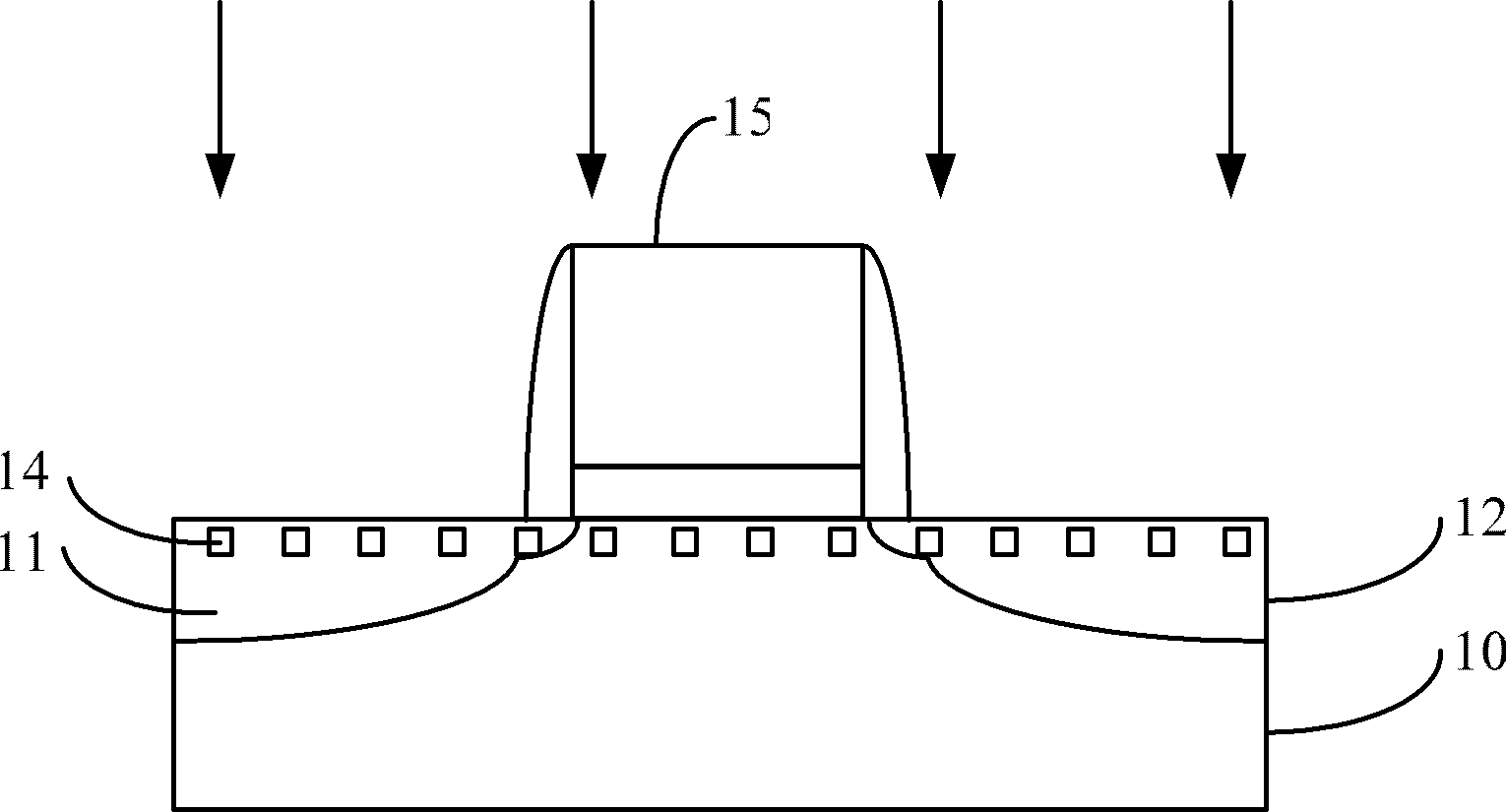
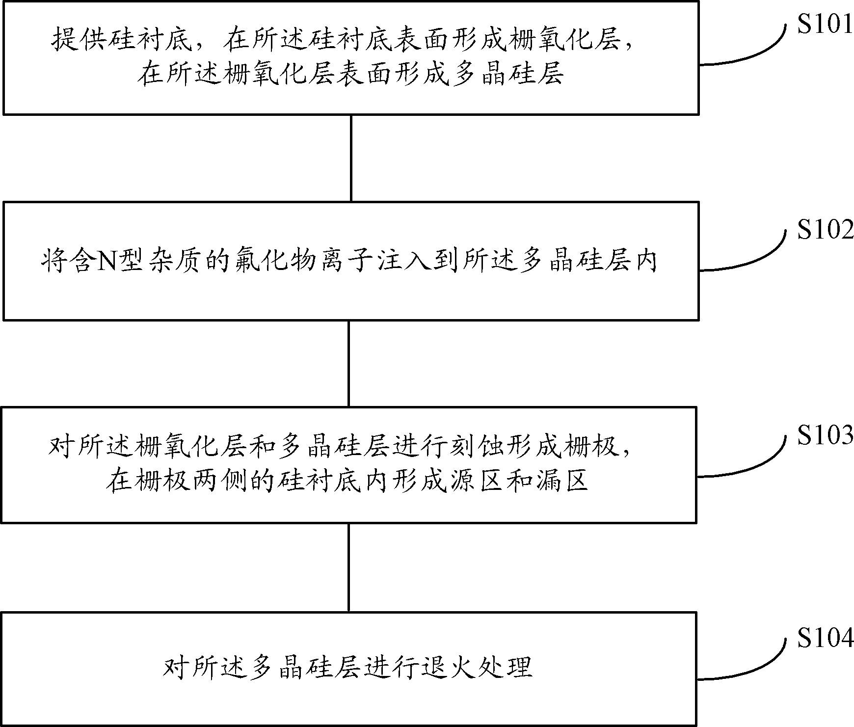
[0029] Since the fluorine ions implanted into the surface layer of the silicon substrate in a large dose will re-form fluorine molecules and escape from the silicon substrate during the annealing process, the inventors have found through research that during the manufacturing process of the NMOS structure, by adding N-type impurities Fluoride is implanted into the polysilicon layer, and then annealing is used to diffuse fluorine ions to the surface of the silicon substrate, so that the fluoride ions combine with silicon on the surface of the silicon substrate to form a silicon-fluorine bond with a large bond energy, which blocks the heat-carrying current in the channel Carriers enter the gate oxide layer, which greatly alleviates the hot carrier injection effect.

[0030] In order to make the above objects, features and advantages of the present invention more comprehensible, specific implementations of the present invention will be described in detail below in conjunction with...


PUM


Abstract

The invention discloses an NMOS (N-Channel Metal Oxide Semiconductor) transistor forming method, which comprises the steps of: providing a silicon substrate, forming a gate oxide on the surface of the silicon substrate, and forming a polycrystalline silicon layer on the surface of the gate oxide; performing ion injecting on a fluoride containing N-type impurity in the polycrystalline silicon layer; etching the gate oxide and the polycrystalline silicon layer to form a grid electrode, and forming a source region and a drain region in the silicon substrates on the two sides of the grid electrode; and annealing the polycrystalline silicon layer. The invention further provides a corresponding COMOS structure forming method. The fluorinion in the polycrystalline silicon layer is diffused to the surface layer of the substrate through annealing treatment and is combined with the silicon to form a silicon-fluorin bond so as to relieve the hot carrier injection effect of the NMOS transistor, and the fluorinion is injected in the substrate in the diffusion mode so as not to be easily changed into gas to escape during the annealing process, so that the dosage of the fluorinion diffused to the substrate can be high.

Description

technical field [0001] The invention relates to semiconductor manufacturing technology, in particular to a method for forming an NMOS transistor capable of reducing the hot carrier injection effect of the NMOS transistor and a corresponding method for forming a CMOS structure. Background technique [0002] With the continuous improvement of the integration level of semiconductor devices, the feature size is gradually reduced, and the length of the channel of the MOS transistor is also gradually reduced. At the same time, both the input / output devices as the peripheral circuits of the chip and the core devices as the memory require a high driving voltage, which causes the electric field in the channel of these devices to become very strong, causing the carriers to collide during the transport process. Ionization generates additional hole-electron pairs, generating hot carriers, and the longitudinal voltage causes some hot carriers to inject into the gate oxide layer, which ca...

Claims


Application Information

Patent Timeline
Patent Type & Authority Patents(China)
IPC IPC(8): H01L21/336H01L21/8238
Inventor 甘正浩冯军宏
Owner SEMICON MFG INT (SHANGHAI) CORP
Why Eureka
Try Eureka