


Quick Research
Generate reliable direction feasibility study reports for your R&D in just a few steps.

Technical Q&A
Discover and master advanced knowledge NOW. Basics, ideas, possibilities, all at once.

Find Solutions
As an expert in R&D theories, this can generate solutions to your technical problems instantly.

Evaluate Feasibility
Analyze your overall solution with one click, know your potential R&D risks in advance.

Monitor Landscape
Get weekly tech updates, stay abreast of the latest tech innovations and key insights.
Wave-absorbing device
A technology of electromagnetic waves and artificial microstructures, applied in electrical components, magnetic field/electric field shielding, etc., can solve problems such as delays and interference with the normal operation of electronic diagnosis and treatment instruments.
- Summary
- Abstract
- Description
- Claims
- Application Information
AI Technical Summary
Problems solved by technology
Method used
Image


Examples
no. 1 example
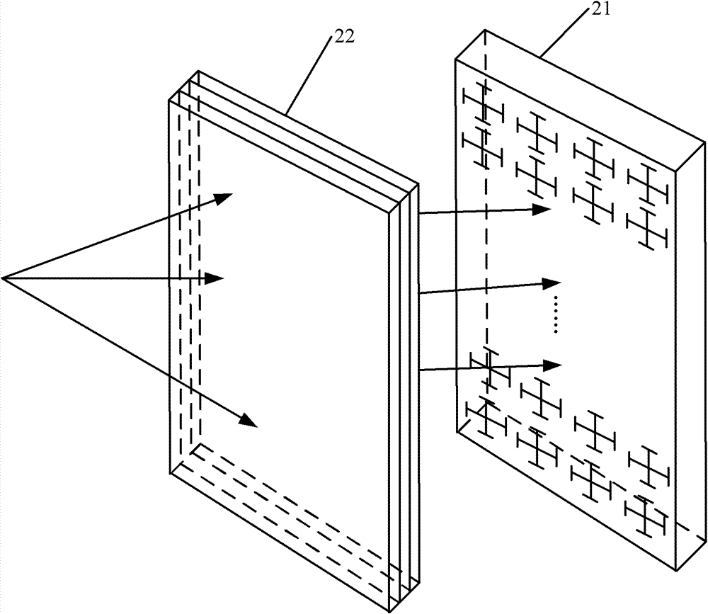
[0016] see figure 2 , the first embodiment of a wave absorbing device in the embodiment of the present invention includes:
[0017] The wave absorbing device includes a wave absorbing module 21 and an electromagnetic wave angle adjustment module 22, wherein the electromagnetic wave angle adjustment module 22 converts the spherical electromagnetic wave emitted by the point source into a plane electromagnetic wave, and the beams of the plane electromagnetic wave are parallel to each other, and the equiphase plane is a plane. The plane electromagnetic wave is incident on the wave absorbing module and absorbed by the wave absorbing module. The electromagnetic wave angle adjustment module includes at least one piece of non-uniform metamaterial. The refractive index of the non-uniform metamaterial gradually decreases from the center along the radial direction to form a circular distribution.
[0018] In this embodiment, by adding an electromagnetic wave angle adjustment module in t...
PUM
 Abstract
Description
Claims
Application Information
 - R&D Engineer
- R&D Manager
- IP Professional
- Industry Leading Data Capabilities
- Powerful AI technology
- Patent DNA Extraction
Browse by: Latest US Patents, China's latest patents, Technical Efficacy Thesaurus, Application Domain, Technology Topic, Popular Technical Reports.
© 2024 PatSnap. All rights reserved.Legal|Privacy policy|Modern Slavery Act Transparency Statement|Sitemap|About US| Contact US: help@patsnap.com