Switching circuit device and power supply device having same
A technology for switching circuits and power supply devices, applied in the direction of output power conversion devices, electrical components, electronic switches, etc., which can solve the problems of high turn-on resistance and increased loss, and achieve the effect of low turn-on resistance and rapid change suppression
- Summary
- Abstract
- Description
- Claims
- Application Information
AI Technical Summary
Problems solved by technology
Method used
Image
Examples
Embodiment Construction
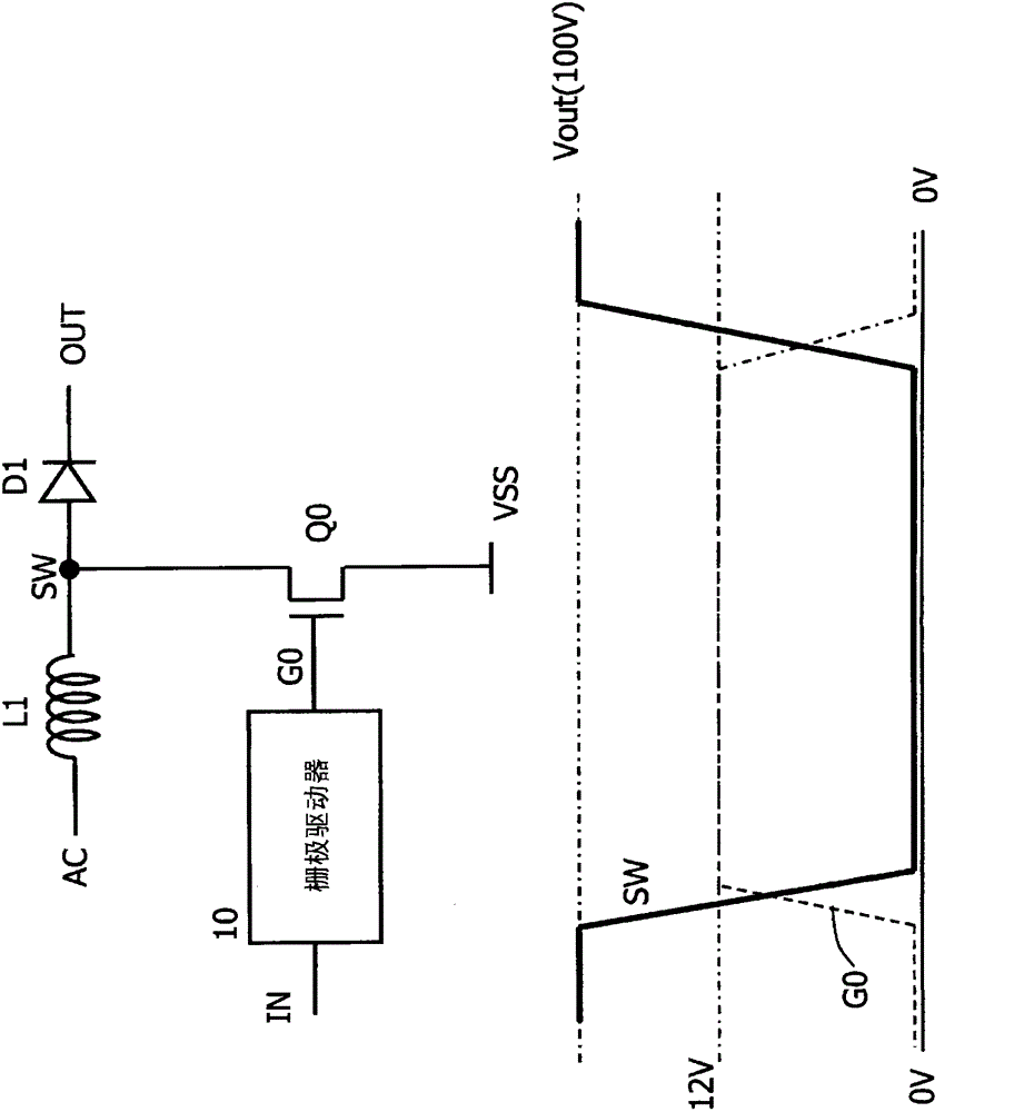
[0017] figure 1 The circuit and operation waveforms of the power supply device with the switching circuit device are shown. The power supply device has: an inductor L1 coupled to an AC power source AC; a diode D1 (which is a unidirectional element) provided between the inductor L1 and an output OUT; and a connection node (first node) SW connecting the inductor L1 and Diode D1. The power supply device also has: a switching transistor Q0 provided between the first node SW and a second node (ground) or another reference power supply VSS; and a gate driver 10 generating a gate voltage applied to the switching transistor Q0 according to a control signal IN. Pole drive signal G0. The switching transistor Q0 is a high-voltage power transistor to which a high voltage is applied, and it turns on and off a large current flowing in the inductor L1. In this example, an N-channel MOSFET is used.
[0018] As shown in the operation waveform diagram, when the gate driver 10 raises the dri...
PUM
 Abstract
Description
Claims
Application Information
 - R&D
- Intellectual Property
- Life Sciences
- Materials
- Tech Scout
- Unparalleled Data Quality
- Higher Quality Content
- 60% Fewer Hallucinations
Browse by: Latest US Patents, China's latest patents, Technical Efficacy Thesaurus, Application Domain, Technology Topic, Popular Technical Reports.
© 2025 PatSnap. All rights reserved.Legal|Privacy policy|Modern Slavery Act Transparency Statement|Sitemap|About US| Contact US: help@patsnap.com


