Method and device for obtaining a multicrystalline semiconductor material, in particular silicon

A semiconductor and equipment technology, applied in the direction of polycrystalline material growth, lighting and heating equipment, crystal growth, etc., can solve problems such as increasing energy consumption levels, increasing costs, and the overall size of furnaces, high energy consumption, etc.

Inactive Publication Date: 2012-10-17
赛亚特股份有限公司
View PDF4 Cites 16 Cited by
  • Summary
  • Abstract
  • Description
  • Claims
  • Application Information

AI Technical Summary

Problems solved by technology

In existing DSS furnaces, which are heated by resistance or induction, this is achieved with heavy insulation layers which increase the cost and overall size of the furnace and therefore increase the energy consumption to control it Level
Additionally, the melting step of the solid semiconducting material to be refined requires long hours and high levels of energy consumption

Method used


Image

  • Method and device for obtaining a multicrystalline semiconductor material, in particular silicon
  • Method and device for obtaining a multicrystalline semiconductor material, in particular silicon
  • Method and device for obtaining a multicrystalline semiconductor material, in particular silicon

Examples


Embodiment Construction

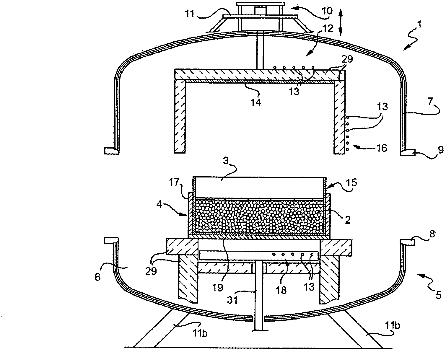
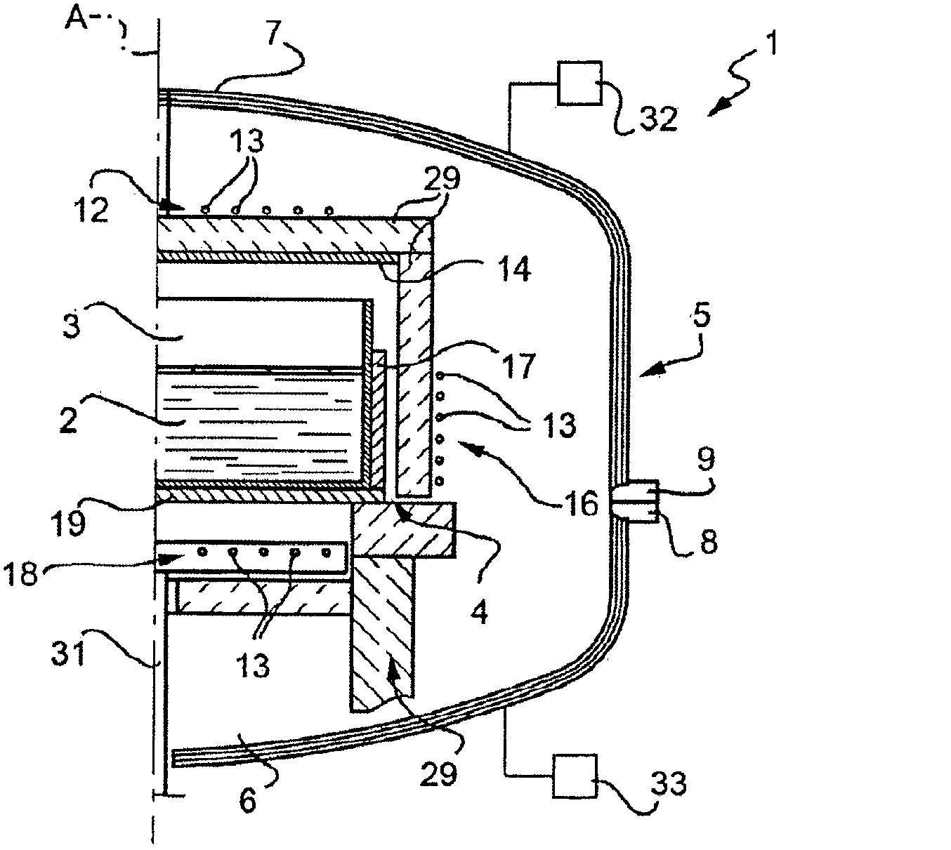
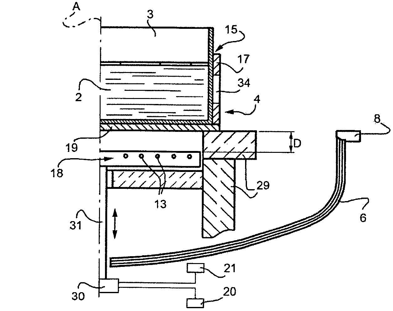
[0026] refer to Figure 1-Figure 4 , 1 collectively designates the equipment for the melting and subsequent directional solidification of semiconductor material 2, typically obtaining polysilicon of solar purity grade.

[0027] The apparatus 1 comprises: at least one crucible 3 for semiconductor material 2, preferably made of quartz or ceramic material, removably arranged in a cup-shaped graphite container 4; and a fluid-tight enclosure 5, in which the graphite container 4 is arranged , the fluid-tight casing 5 is bounded by a lower half-shell 6 and an upper half-shell 7, both cup-shaped; these shells are preferably made of steel and are usually connected up and down relative to each other ( figure 2 ), their concavities facing each other, the respective edges 8, 9 with appropriate gaskets (not shown) abut together in a fluid-tight manner.

[0028] The device 1 also comprises means 10 for vertically moving the upper half-shell 7 away from the lower half-shell 6, in this case...


PUM


Abstract

A device (1) for obtaining multicrystalline silicon, including: at least one crucible (3) made of quartz for the silicon, removably housed in a cup-shaped graphite container (4); a fluid-tight casing (5), including a fixed bottom half-shell (6) and a vertically mobile top half-shell (7); a top induction coil (12), set facing, with interposition of a graphite plate (14), the crucible, a lateral induction coil (16), set around a side wall (17) of the graphite container, and a bottom induction coil (18), set facing a bottom wall (19) of the graphite container and vertically mobile for varying the distance (D) from the bottom wall; and means (20) for a. c. electrical supply of the induction coils separately from one another; at least the lateral induction coil (16) includes a plurality of plane turns (13a...13e) set on top of one another, and means (25) for selectively short-circuiting, supplying or not supplying the turns, all together or separately one or more at a time and for varying the frequency of supply thereof all together or separately one or more at a time.

Description

technical field [0001] The invention relates to a method and a device for obtaining polycrystalline semiconductor material, in particular silicon, by melting the semiconductor material and its subsequent directional solidification. Background technique [0002] There is an increasing demand for semiconductor materials, especially silicon, with a high purity level known as "solar purity", since said materials are necessary for the production of high efficiency photovoltaic cells. [0003] To obtain the material, it is first refined through traditional metallurgical methods and finally formed into ingots, from which the wafers needed to produce photovoltaic cells are cut. The ingot is formed using a method known as the "Directional Solidification System" (DSS), ie by melting the semiconductor material in a crucible and then directional solidifying it to finally obtain polysilicon. [0004] In order to achieve directional solidification, it is necessary to achieve the solidifi...

Claims


Application Information

Patent Timeline
Patent Type & Authority Applications(China)
IPC IPC(8): C30B11/00B22D27/04F27B14/14H05B6/36H05B6/44C30B29/06C30B35/00
CPCF27B14/14H05B6/367C30B29/06H05B6/24H05B6/36H05B6/44C30B35/00C30B11/003B22D27/045B22D27/04C30B11/00
Inventor 发布里奇奥·杜吉罗米歇尔·福尔赞达里奥·齐斯卡托马里奥力诺·切萨诺发布里奇奥·克里韦洛保罗·贝尔纳比尼
Owner 赛亚特股份有限公司
Why Eureka
Try Eureka