Method for manufacturing quantum dot field effect transistor array

A technology of field-effect transistors and quantum dots, which is applied in the field of weak light detection, can solve the problems that ordinary CCDs cannot effectively detect weak light, and achieve the effects of low power consumption, low working voltage and high detection efficiency

Inactive Publication Date: 2012-10-17
INST OF SEMICONDUCTORS - CHINESE ACAD OF SCI
View PDF4 Cites 7 Cited by
  • Summary
  • Abstract
  • Description
  • Claims
  • Application Information

AI Technical Summary

Problems solved by technology

[0005] In view of this, the main purpose of the present invention is to provide a method for preparing a quantum dot field effect transistor array, to solve the problem that ordinary CCDs cannot effectively detect weak light, achieve low power consumption, and realize image processing under weak light conditions. capture of high-gain low-light detection purposes

Method used


Image

  • Method for manufacturing quantum dot field effect transistor array
  • Method for manufacturing quantum dot field effect transistor array
  • Method for manufacturing quantum dot field effect transistor array

Examples


Embodiment Construction

[0034] In order to make the object, technical solution and advantages of the present invention clearer, the present invention will be described in further detail below in conjunction with specific embodiments and with reference to the accompanying drawings.

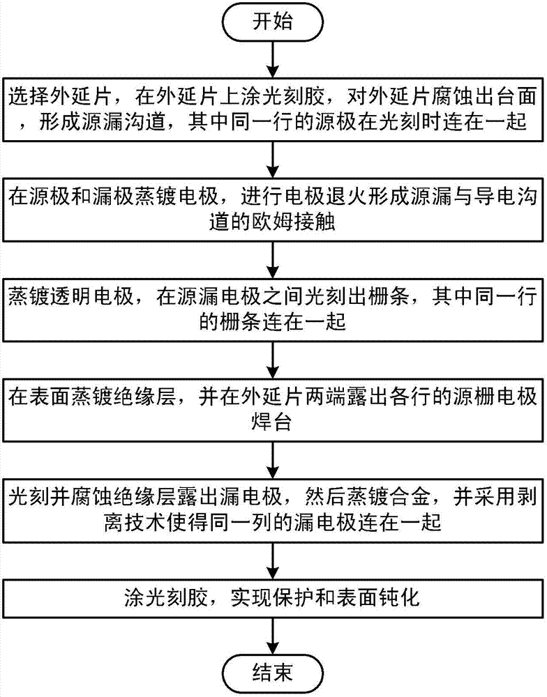
[0035] like figure 1 as shown, figure 1 It is a flowchart of a method for preparing a quantum dot field effect transistor array according to an embodiment of the present invention, and the method includes the following steps:

[0036] Step 1: Select the epitaxial wafer, apply photoresist on the epitaxial wafer, etch the epitaxial wafer to form a source-drain channel, and the sources of the same row are connected together during photolithography;

[0037] Step 2: Evaporate electrodes on the source and drain electrodes, and perform electrode annealing to form ohmic contacts between the source and drain electrodes and the conductive channel;

[0038] Step 3: Evaporate transparent electrodes, and photo-etch grid strips betw...


PUM

PropertyMeasurementUnit
Thicknessaaaaaaaaaa
Thicknessaaaaaaaaaa
Thicknessaaaaaaaaaa

Abstract

The invention discloses a method for manufacturing a quantum dot field effect transistor array. The method comprises the following steps of: selecting an epitaxial wafer, coating photoresist on the epitaxial wafer to corrode the epitaxial wafer to form a table board to form a source-drain channel, wherein sources in a same row are connected together during photoetching; evaporating an electrode on a source and a drain to carry out electrode annealing to form ohmic contact of the source, the drain and a conductive channel; evaporating a transparent electrode to photoetch grids between the source and the drain, wherein the grids in the same row are connected together; evaporating an insulating layer on the surface and exposing source-grid electrode welding tables at each row and at two ends of the epitaxial wafer; photoetching and corroding the insulating layer to enable the drain to be exposed, evaporating alloy, and utilizing a stripping technique to enable the drains at a same column to be connected together; and coating the photoresist to realize protection and surface passivation. Through the method for manufacturing the quantum dot field effect transistor array, disclosed by the invention, a problem that the common CCD (charge coupled device) can not effectively perform low-light detection is solved, the power consumption is low, and a purpose of high-gain low-light detection of image capture is realized under a weak light condition.

Description

technical field [0001] The present invention relates to the technical field of weak light detection, and specifically refers to a method for preparing a quantum dot field effect transistor array that can be used for weak light imaging detection. High-gain low-light detector array for image capture. Background technique [0002] Weak light detection has a wide range of applications, in the fields of high-resolution spectral measurement, non-destructive material analysis, high-speed phenomenon detection, precision analysis, air pollution, bioluminescence, radiation detection, high-energy physics, astrophotometry, optical time-domain reflectometry, etc. have been applied. The planar low-light detection array has been widely concerned because of its ability to obtain image information. [0003] A general photodetection planar array uses a charge-coupled device (CCD) to read and analyze images. When the light shines on the MOS device in the deep depletion state, the light is c...

Claims


Application Information

Patent Timeline
IPC IPC(8): H01L27/146B82Y10/00
Inventor 聂诚磊杨晓红王秀平王杰刘少卿李彬杨怀伟尹伟红韩勤
Owner INST OF SEMICONDUCTORS - CHINESE ACAD OF SCI
Why Eureka
Try Eureka