X-ETFE (crosslinked ethylene-tetrafluoroethylene) insulating wire or cable with spiral stripe identifications for aerospace and preparation process for insulating wire or cable
An X-ETFE, aerospace technology, used in insulated cables, marked conductors/cables, insulated conductors, etc., to achieve good UV resistance and reduce vehicle weight
- Summary
- Abstract
- Description
- Claims
- Application Information
AI Technical Summary
Problems solved by technology
Method used
Image
Examples
Embodiment 1
[0030] Such as figure 1 As shown, it is a schematic structural diagram of the spiral stripe marking wire (including a single insulated core wire, without a sheath layer) of the present invention, and the conductor 1 formed by twisting is covered with a double-layer insulation layer composed of an inner and outer insulation layer. Layer 2, with a spiral stripe logo 3 printed on the outside of the insulating layer 2;
[0031] Its preparation process is as follows:
[0032] 1) Conductor stranding: use annealed silver-plated (nickel) copper conductors for stranding with a pitch ratio of less than 20;
[0033] 2) Insulation layer extrusion: inner and outer insulation layers are co-extruded (extrusion temperature is 245-315°C) to form a double-layer insulation layer. The rubber material of the insulation layer is X-ETFE, and the concentricity of the insulation layer is 85%. The thinnest point of the layer is 0.08mm, and the thinnest point of the outer insulating layer is 0.10mm; ...
Embodiment 2
[0039] Such as figure 2 As shown, it is a structural schematic diagram of the spiral stripe marking cable (composed of a single insulated core wire, a shielding layer and a sheath layer) of the present invention, the conductor 1 formed by twisting is covered with an insulating layer 2, and the insulating layer 2 is provided with a shielding layer 3 outside, and a sheath layer 4 is covered outside the shielding layer 3, and a spiral stripe logo 5 is printed on the sheath layer 4.
[0040] Its preparation process is as follows:
[0041] 1) Conductor stranding: use annealed silver-plated (nickel) copper conductors for stranding with a pitch ratio of less than 20;
[0042] 2) Extrusion of insulating layer: high-temperature extrusion of single-layer insulation (extrusion temperature is 245-300°C), the compound of the insulating layer is X-ETFE, the concentricity of the insulating layer is 85%, and the thinnest point of the insulating layer is 0.13mm;
[0043] 3) Carry out radiat...
Embodiment 3
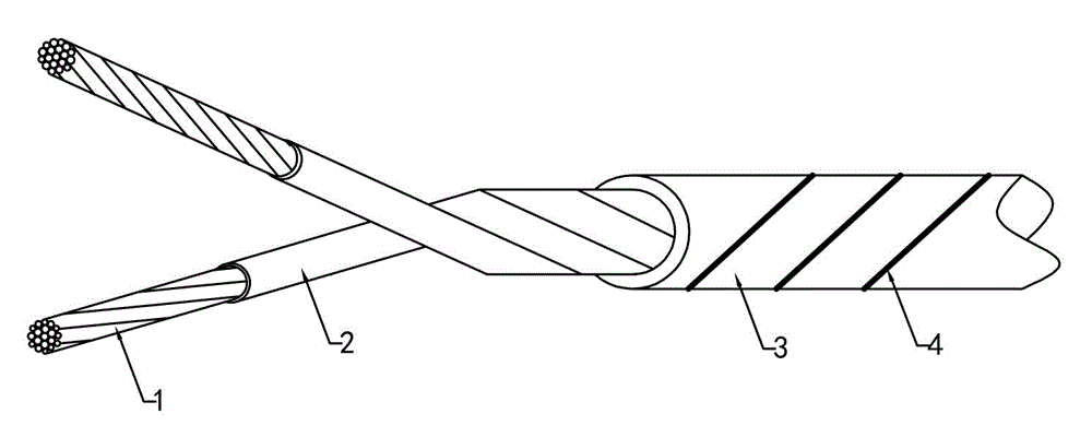
[0051] Such as image 3 As shown, it is a structural schematic diagram of the spiral striped marking cable (composed of two insulated core wires and a sheath layer) of the present invention, the conductor 1 formed by twisting is covered with an insulating layer 2, and the conductor 1 and the insulating layer 2 An insulated core wire is formed, and the insulating layer 2 is covered with a sheath layer 3 , and a spiral stripe logo 4 is printed on the surface of the sheath layer 3 .
[0052] Its preparation process is as follows:
[0053] 1) Conductor stranding: use annealed silver-plated (nickel) copper conductors for stranding with a pitch ratio of less than 20;
[0054] 2) Extrusion of insulating layer: high-temperature extrusion of single-layer insulation (extrusion temperature is 245-300°C), the compound of the insulating layer is X-ETFE, the concentricity of the insulating layer is 83%, and the thinnest point of the insulating layer is 0.13mm;
[0055] 3) Carry out radiat...
PUM
| Property | Measurement | Unit |
|---|---|---|
| tensile strength | aaaaa | aaaaa |
| flame retardant | aaaaa | aaaaa |
| flame retardant | aaaaa | aaaaa |
Abstract
Description
Claims
Application Information
 - Generate Ideas
- Intellectual Property
- Life Sciences
- Materials
- Tech Scout
- Unparalleled Data Quality
- Higher Quality Content
- 60% Fewer Hallucinations
Browse by: Latest US Patents, China's latest patents, Technical Efficacy Thesaurus, Application Domain, Technology Topic, Popular Technical Reports.
© 2025 PatSnap. All rights reserved.Legal|Privacy policy|Modern Slavery Act Transparency Statement|Sitemap|About US| Contact US: help@patsnap.com


