
High-frequency intelligent label chip with built-in antenna

A technology with built-in antenna and smart label, which is applied to record carriers, instruments, computer parts, etc. used in machines, can solve the problems of lower product cost performance, lower product quality, and affect production process, so as to save production materials and reduce production costs. , to avoid the effect of quality degradation

Inactive Publication Date: 2012-08-29
上海祯显电子科技有限公司
View PDF1 Cites 4 Cited by
  • Summary
  • Abstract
  • Description
  • Claims
  • Application Information

AI Technical Summary

Problems solved by technology

During the surface mount process, it is easy to contaminate the solder to the chip pad, and the high-temperature baking process of reflow soldering will cause oxidative denaturation of the coating on the surface of the substrate and changes in the physical size of the substrate, especially the deformation of the substrate, which will easily affect subsequent production process, resulting in a decline in product quality
Increased capacitors and surface mount technology will increase the cost, reduce the cost performance of the product, and affect the overall competitiveness of the product
Most importantly, there is a physical connection between the antenna and the chip, so the overall size quotient cannot achieve true miniaturization

Method used


Image

  • High-frequency intelligent label chip with built-in antenna
  • High-frequency intelligent label chip with built-in antenna
  • High-frequency intelligent label chip with built-in antenna

Examples


Embodiment Construction

[0028] In order to make it easy to understand the technical means, creation features, achieved goals and effects of the present invention, the present invention will be further described below with reference to the specific figures.

[0029] Aiming at the problems of the production process commonly used in the existing miniature smart labels, the present invention not only has high production cost, but also has a cumbersome manufacturing process, relatively poor reliability in use, and large product volume. as follows:

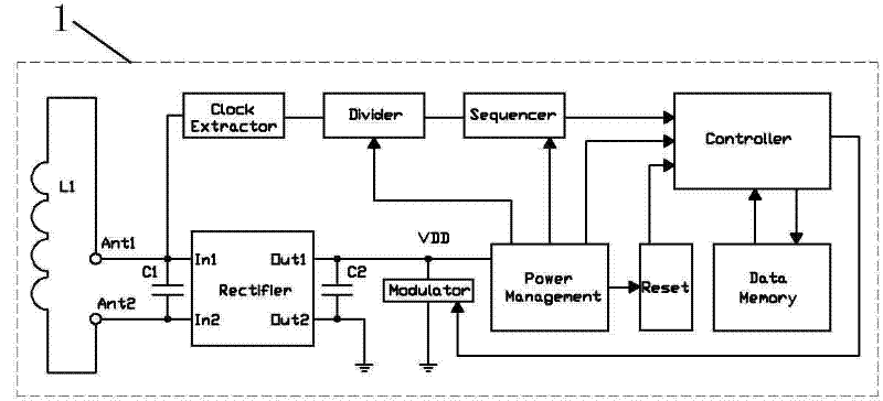
[0030] see figure 2 The internal structure, working principle block diagram and application schematic diagram of the traditional high-frequency smart tag chip. The part within the dotted box 1 is the chip body, which is composed of the input capacitor C1, the rectifier circuit Rectifier and the signal processing circuit. The input capacitor C1 is an equivalent capacitor arranged on the semiconductor substrate, and its capacity is between 10 and 30pF, and oc...


PUM


Abstract

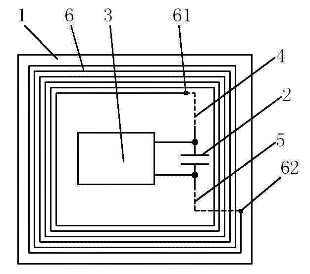
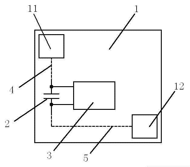
The invention discloses a high-frequency intelligent label chip with a built-in antenna, which comprises the high-frequency antenna, an input capacitor, a rectification circuit and a signal processing circuit. The high-frequency antenna is a multi-turn square hollow conductive induction coil which is arranged on a semiconductor substrate by the photoetching process, and the coil is arranged along the edge of the chip and around the center; the input capacitor is an equivalent capacitor which is arranged on the semiconductor substrate and connected in parallel with the high-frequency antenna; the rectification circuit is a four-port input / output circuit, the two input ports are connected with the ports of the high-frequency antenna, and the two output ports are chip interior power supply ports, one of which is VDD and the other of which is GND; and the signal processing circuit comprises a central control circuit, a data memory circuit, a clock circuit, a modulation / demodulation circuit, a frequency-dividing circuit, a power management circuit and a resetting circuit. Consequently, the intelligent label chip has an independent high-frequency radio frequency communication function.

Description

technical field [0001] The invention relates to the field of high-frequency radio frequency communication and the field of high-frequency smart label chips, in particular to a high-frequency smart label chip with a built-in antenna. Background technique [0002] In recent years, due to the continuous development of radio frequency electronic technology, especially the wide application of radio frequency smart labels, people's way of life is gradually changing. Common radio frequency electronic tags are divided into two categories: active and passive in terms of power supply; in terms of carrier frequency, there are 125KHz (130KHz) low-frequency bands, 13.56MHz high-frequency bands, 433MHz, 915MHz ultra-high frequency bands , 2.4GHz, 5.8GHz microwave frequency band; the application of electronic tags is ubiquitous, so there are various shapes and products suitable for different application requirements, making people's life more convenient and efficient. [0003] The convent...

Claims


Application Information

Patent Timeline
Patent Type & Authority Applications(China)
IPC IPC(8): G06K19/077
Inventor 陆红梅
Owner 上海祯显电子科技有限公司
Learn More