Method for producing silicon doping zinc oxide film, produced film and application thereof
A zinc oxide thin film, silicon doping technology, applied in the direction of final product manufacturing, sustainable manufacturing/processing, vacuum evaporation plating, etc., can solve the problems of increased resistivity and decreased crystal quality of the film, and achieve the reduction of resistivity, Good film adhesion and high deposition rate
- Summary
- Abstract
- Description
- Claims
- Application Information
AI Technical Summary
Problems solved by technology
Method used
Image


Examples
preparation example Construction
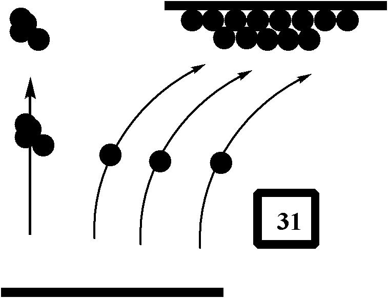
[0018] see figure 1 , showing a method for preparing a silicon-doped zinc oxide film according to an embodiment of the present invention, which includes the following steps:
[0019] SiO 2 Powder and ZnO powder are mixed and sintered as SZO target material, the SiO 2 The mass ratio of the powder to the ZnO powder is 1 / 199-1 / 66;
[0020] Put the SZO target into the magnetron sputtering chamber, vacuumize, set the working pressure to 0.2Pa~1.5Pa, the inert gas flow rate to 15sccm~25sccm, the substrate temperature to 300℃~800℃, the sputtering of the SZO layer The radiation power is 45W ~ 300W, and the electromagnetic field is applied in the direction perpendicular to the flying direction of the sputtering particles. The number of coil turns in the electromagnetic field is 50N ~ 500N, and the coil area is 15cm 2 ~80cm 2 , the excitation current is 0.1A-5A, and the silicon-doped zinc oxide film is sputtered on the substrate.
[0021] In step S01, the SiO 2 Mix the powder and ...
Embodiment 1
[0028] Choose SiO with a purity of 99.9% 2 The mass ratio of powder and ZnO powder is 1:99. After uniform mixing, they are sintered at 1000°C to form a Φ50×2mm ceramic target, and the target is loaded into a vacuum chamber. Then, the quartz substrate was ultrasonically cleaned with acetone, absolute ethanol and deionized water, dried with high-purity nitrogen, and placed in a vacuum chamber. The distance between the target and the substrate is set to 60mm. Use a mechanical pump and a molecular pump to evacuate the cavity to 6.0×10 -4 Pa, 20 sccm of argon gas was introduced, the pressure was adjusted to 1.0 Pa, the substrate temperature was set to 450°C, and the sputtering power was adjusted to 60W. Apply a magnetic field electric coil on the vertical surface of the base target, the number of coil turns is 300N, and the coil area is 50cm 2 , the excitation current is 3.5A, and the film deposition starts. The resistivity of the obtained film is 3.9×10 -4 Ω·cm.
Embodiment 2
[0030] Choose SiO with a purity of 99.9% 2 The mass ratio of powder and ZnO powder is 1:99. After uniform mixing, they are sintered at 1000°C to form a Φ50×2mm ceramic target, and the target is loaded into a vacuum chamber. Then, the quartz substrate was ultrasonically cleaned with acetone, absolute ethanol and deionized water, dried with high-purity nitrogen, and placed in a vacuum chamber. The distance between the target and the substrate is set to 60mm. Use a mechanical pump and a molecular pump to evacuate the cavity to 6.0×10 -4 Pa, 20 sccm of argon gas was introduced, the pressure was adjusted to 1.0 Pa, the substrate temperature was set to 450°C, and the sputtering power was adjusted to 80W. Apply a magnetic field electric coil on the vertical surface of the base target, the number of coil turns is 300N, and the coil area is 50cm 2 , the excitation current is 2.5A, and the film deposition starts. The resistivity of the obtained film is 8.8×10 -4 Ω·cm.
PUM
| Property | Measurement | Unit |
|---|---|---|
| electrical resistivity | aaaaa | aaaaa |
| area | aaaaa | aaaaa |
| thickness | aaaaa | aaaaa |
Abstract
Description
Claims
Application Information
 - R&D
- Intellectual Property
- Life Sciences
- Materials
- Tech Scout
- Unparalleled Data Quality
- Higher Quality Content
- 60% Fewer Hallucinations
Browse by: Latest US Patents, China's latest patents, Technical Efficacy Thesaurus, Application Domain, Technology Topic, Popular Technical Reports.
© 2025 PatSnap. All rights reserved.Legal|Privacy policy|Modern Slavery Act Transparency Statement|Sitemap|About US| Contact US: help@patsnap.com