
A switching power supply power compensation circuit and power supply chip

A switching power supply circuit and power compensation technology, which is applied in the direction of high-efficiency power electronic conversion, output power conversion device, electrical components, etc., can solve the problems of many pins, poor compensation effect, low efficiency, etc., and achieve the design value and actual value The effect of small deviation, compensating output power and reducing system efficiency

Inactive Publication Date: 2016-05-25
深圳鼎信芯微电子有限公司
View PDF4 Cites 0 Cited by
  • Summary
  • Abstract
  • Description
  • Claims
  • Application Information

AI Technical Summary

Problems solved by technology

[0011] The purpose of the embodiment of the present invention is to provide a switching power supply power compensation circuit, which aims to solve the problems of the existing power compensation circuit with many pins, low efficiency and poor compensation effect

Method used


Image

  • A switching power supply power compensation circuit and power supply chip
  • A switching power supply power compensation circuit and power supply chip
  • A switching power supply power compensation circuit and power supply chip

Examples


Embodiment Construction

[0031] In order to make the object, technical solution and advantages of the present invention clearer, the present invention will be further described in detail below in conjunction with the accompanying drawings and embodiments. It should be understood that the specific embodiments described here are only used to explain the present invention, not to limit the present invention.

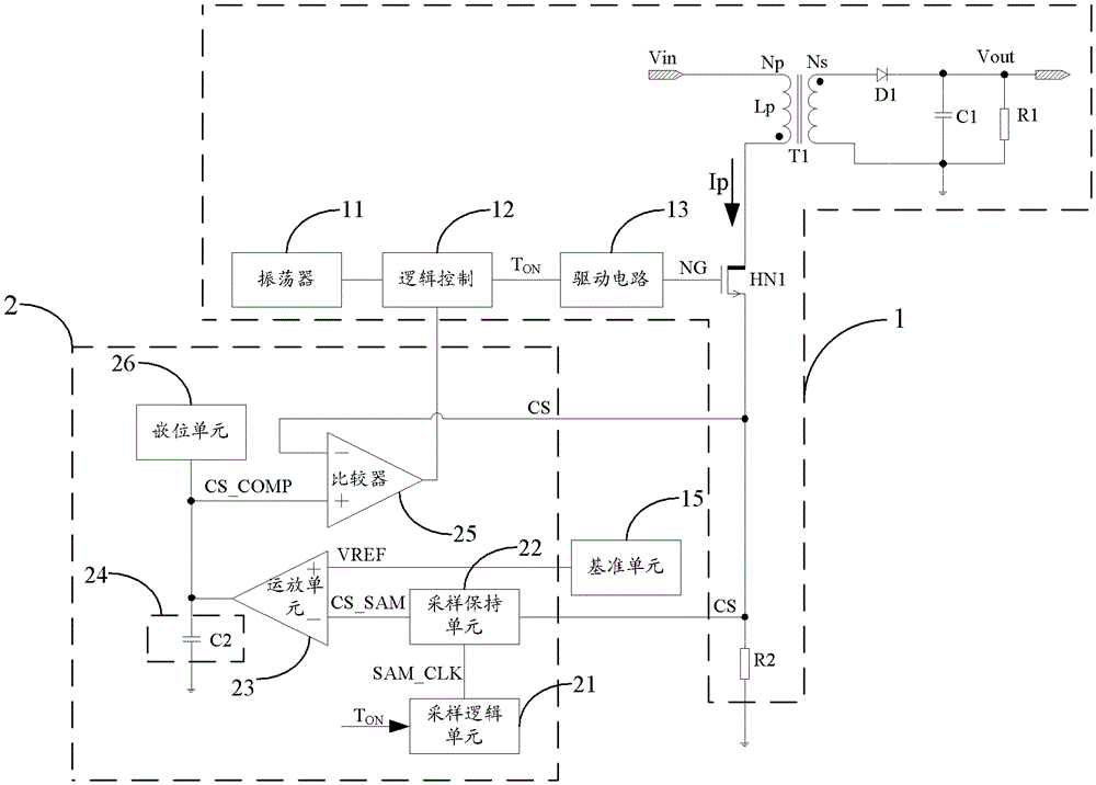
[0032] The embodiment of the present invention controls the peak current on the primary inductor Lp through a negative feedback loop, and increases the loop gain, precisely optimizes the sampling time point, and compensates the output power without adding additional chip pins and reducing system efficiency.

[0033] figure 2 The structure of the switching power supply power compensation circuit provided by the embodiment of the present invention is shown, and for the convenience of description, only the parts related to the present invention are shown.

[0034] The switching power supply circuit ...


PUM


Abstract

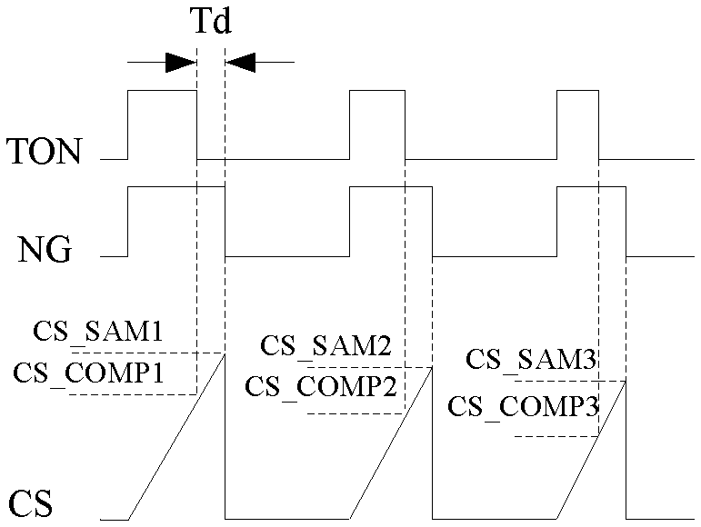
The invention is suitable for the field of integrated circuits and provides a power compensation circuit and a power supply chip of a switching power supply. The power compensation circuit comprises a sampling logic unit, a sampling retaining unit, an operational amplification unit, an energy accumulation unit, a comparator and a clamping unit, wherein the sampling logic unit is used for generating a sampling control signal according to a logic control signal; the sampling retaining unit is used for outputting a sampling processing unit according to the sampling control signal; the operational amplification unit is used for outputting an error amplification signal according to the sampling processing signal and a reference signal; the energy accumulation unit is used for charging and discharging according to the error amplification signal so as to adjust the voltage of the error amplification signal; the comparator is used for comparing a sampling voltage with the adjusted error amplification signal and outputting a compensation control signal so as to compensate peak current of a primary inductor and further compensate power; and the clamping unit is used for clamping the error compensation signal. In the invention, the peak current of the primary inductor is controlled through a negative feedback loop, and the loop gain is increased, thus the sampling time point is precisely optimized, and the output power is compensated on the basis that chip pins are not additionally increased and system efficiency is reduced.

Description

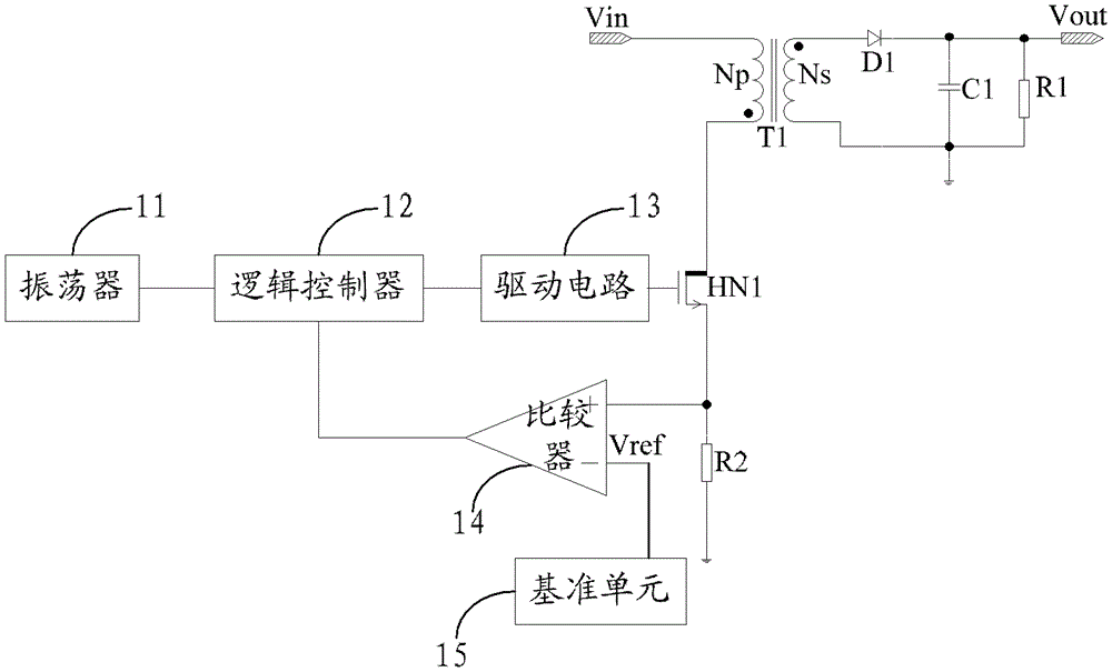
technical field [0001] The invention belongs to the field of integrated circuits, in particular to a switching power supply power compensation circuit and a power supply chip. Background technique [0002] At present, in switching power supplies, since the range of AC input voltage usually varies between 85VAC and 265VAC, and there is a certain delay in the control system, the maximum output power will have a large deviation under different input voltages, which is not conducive to precise control . [0003] Taking the flyback switching power supply as an example, figure 1 It shows the structure of the existing flyback control switching power supply maximum output power circuit, which includes: oscillator 11, logic controller 12, drive circuit 13, comparator 14, transformer T1, first switching tube HN1, diode D1 , capacitor C1, resistor R1 and resistor R2; [0004] The output end of the oscillator 11 is connected to the input end of the logic controller 12, the output end...

Claims


Application Information

Patent Timeline
Patent Type & Authority Patents(China)
IPC IPC(8): H02M3/28H02M1/42
CPCY02B70/10
Inventor 田欢张奇
Owner 深圳鼎信芯微电子有限公司
Learn More