
Preparation method of large-area sequential controllable surface-enhanced Raman active substrate

A surface-enhanced Raman and active substrate technology, applied in Raman scattering, material excitation analysis, etc., can solve the problems of small substrate area, poor substrate repeatability, complex process, etc., achieve orderly and controllable substrate structure, and prepare substrates. Large area and good substrate repeatability

Inactive Publication Date: 2012-08-01
INST OF SEMICONDUCTORS - CHINESE ACAD OF SCI
View PDF10 Cites 25 Cited by
  • Summary
  • Abstract
  • Description
  • Claims
  • Application Information

AI Technical Summary

Problems solved by technology

For the electrochemical redox method and the metal sol method, the substrates prepared generally have problems such as poor repeatability, low stability and complicated preparation process.
Focused ion beam etching and electron beam etching techniques have high etching resolution and pattern making freedom, so metal nanostructure substrates with good repeatability and high stability can be obtained, but these methods are costly, complicated, and The area of ​​the prepared substrate is small and the speed is slow, which cannot realize industrialized mass production
Nanoimprint technology can avoid the above problems, but it needs to make nanostructure imprint templates through fine micro-nano processing technology, and it is not convenient to randomly adjust the structural parameters of fine patterns

Method used


Image

  • Preparation method of large-area sequential controllable surface-enhanced Raman active substrate
  • Preparation method of large-area sequential controllable surface-enhanced Raman active substrate
  • Preparation method of large-area sequential controllable surface-enhanced Raman active substrate

Examples


Embodiment Construction

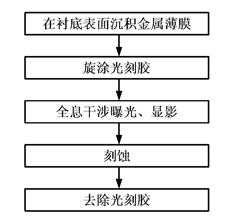
[0020] see figure 1 As shown, the present invention provides a method for preparing a large-area ordered and controllable surface-enhanced Raman active substrate, comprising the following steps:

[0021] Step 1: Take a substrate, the material of which is glass, single crystal Si, sapphire, GaAs or GaN. The taken substrate is cleaned to remove surface impurities. For glass, sapphire, GaAs or GaN substrates, first scrub the polished surface of the substrate with cotton soaked in acetone; place it in acetone and absolute ethanol for 5 minutes (temperature 55°C); Rinse with water 40 times; then soak in acetone and dry with nitrogen to complete the cleaning of the glass substrate. For a single crystal Si substrate, first scrub the polished surface of the substrate with cotton soaked in acetone; place it in acetone and absolute ethanol in sequence for 5 minutes (temperature 55 ° C); rinse with deionized water 40 times; Boil it with a mixed solution of sulfuric acid and hydrogen p...


PUM


Abstract

The invention provides a preparation method of a large-area sequential controllable surface-enhanced Raman active substrate. The preparation method comprises the following steps of: step 1: depositing a metal thin film on the surface of a clean liner by using an electron beam evaporation technology; step 2: spinning a photoresist on the metal thin film and prebaking; step 3: utilizing a holographic interference exposure technology to obtain an imaged photoresist mask plate so as to form a substrate composed of the liner, the metal thin film and the imaged photoresist mask plate; step 4: etching the substrate, wherein the etching depth reaches the surface of the liner; and step 5: removing the residual photoresist to form the large-area sequential controllable surface-enhanced Raman active substrate. The prepared large-area sequential controllable surface-enhanced Raman active substrate prepared by the method has the advantages of large area, sequential and controllable structure, good repeatability, high stability, low manufacturing cost, simplicity in operation and the like.

Description

technical field [0001] The invention belongs to the fields of Raman spectrum analysis and detection technologies such as biosensing, electrochemical monitoring, and environmental analysis, and nanomaterials, and specifically relates to a method for preparing a large-area, orderly, and controllable surface-enhanced Raman active substrate. Background technique [0002] Raman spectroscopy is a molecular structure characterization technique based on the Raman effect. Its signal originates from the transition of molecular vibration and rotational energy levels, and it has broad application prospects in the fields of biomedicine, electrochemical analysis, environmental science, and food safety. However, in general, the Raman scattering cross section of a molecule is about 10-31 cm 2 , so that the Raman signal intensity is only about 10-10 of the incident light intensity. Therefore, people introduce specific enhancement effects to increase the intensity of Raman signals, such as ...

Claims


Application Information

Patent Timeline
IPC IPC(8): G01N21/65
Inventor 宋国峰王立娜张晶白文理蔡立康胡海峰
Owner INST OF SEMICONDUCTORS - CHINESE ACAD OF SCI
Learn More