Bismuthstan silver system lead-free solder
A lead-free solder and silver-based technology, applied in the direction of welding/cutting medium/material, welding medium, welding equipment, etc., can solve the problems of increased production cost of solder
- Summary
- Abstract
- Description
- Claims
- Application Information
AI Technical Summary
Problems solved by technology
Method used
Image
Examples
Embodiment 1
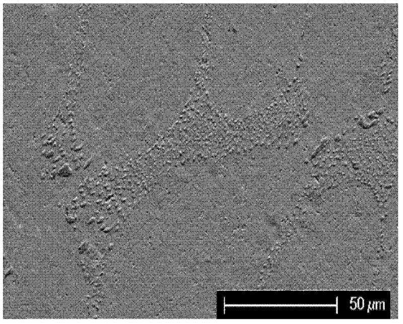
[0017] Take 98.85 grams of tin with a purity of not less than 99.99%, 1.0 grams of bismuth, 0.1 grams of silver, and 0.05 grams of zinc for mixing, heat the mixture to 1100 ° C in a vacuum melting furnace under the protection of argon, and add magnetic stirring. Make the composition of the alloy uniform, and then cool the water-cooled copper mold. Then the alloy is turned over and reheated to 500°C to melt, and at the same time, it is magnetically stirred and cooled by a water-cooled copper mold, and this is repeated at least three times to obtain a solder alloy; the composition is 1.0% Bi-0.1% Ag-0.05% Zn and the matrix is Sn solder alloy. Its microstructure is as figure 1 As shown, the particles are Ag 3 Sn phase, the matrix is Sn.
Embodiment 2
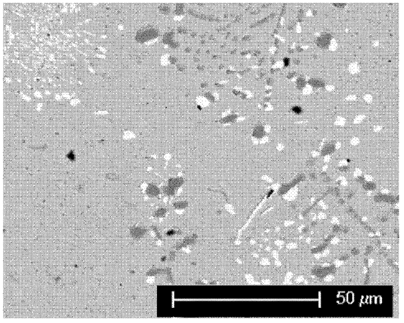
[0019] Take 93.5 grams of tin, 4.0 grams of bismuth, 0.5 grams of silver, 1.0 grams of zinc, and 1.0 grams of copper with a purity of not less than 99.99%, mix them, and heat the mixture to 1100 ° C in a vacuum melting furnace protected by argon. Add magnetic stirring to make the alloy composition uniform, and then cool down in a water-cooled copper mold. Then turn the alloy over and reheat to 500°C to melt, and at the same time add magnetic stirring and water-cooled copper mold to cool down, so repeat at least three times to obtain a solder alloy; the composition is 4.0%Bi-0.5%Ag-1.0%Zn-1.0%Cu The matrix is Sn solder alloy. Its microstructure is as figure 2 As shown, the particles are Ag 3 Sn phase and Cu 6 sn 5 phase, the white particles are Bi, and the matrix is Sn.
Embodiment 3
[0021] Mix tin (98.8-x) gram, bismuth x gram (x=1.0, 2.0, 3.0 or 4.0 gram), silver 0.3 gram, and zinc 0.9 gram with a purity of not less than 99.99%, and place the mixture under argon protection It is heated to 1100°C in the vacuum melting furnace under it, and then magnetically stirred to make the alloy composition uniform, and then the water-cooled copper mold is cooled. The alloy is turned over and reheated to 500°C for melting, while magnetic stirring and cooling of the water-cooled copper mold are performed, so that the solder alloy is obtained at least three times; x%Bi-0.3%Ag-0.9Zn% (x=1.0, 2.0, 3.0 and 4.0) The substrate is a Sn solder alloy.
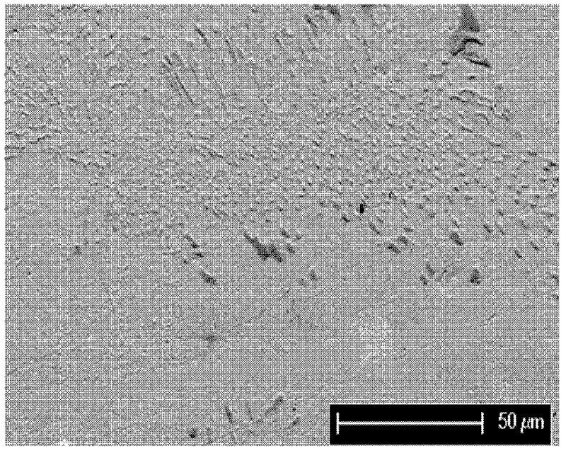
[0022] Among them, the microstructure of Sn-2.0%Bi-0.3%Ag-0.9%Zn solder alloy is as follows image 3 As shown, the particles are Ag 3 In the Sn phase, the white enrichment area is Bi, and the matrix is Sn. The melting curve and stress-strain of Sn-x%Bi-0.3%Ag-0.9%Zn lead-free solder alloy are shown as Figure 4 and Figur...
PUM
| Property | Measurement | Unit |
|---|---|---|
| Melting point | aaaaa | aaaaa |
| Maximum tensile strength | aaaaa | aaaaa |
Abstract
Description
Claims
Application Information
 - R&D Engineer
- R&D Manager
- IP Professional
- Industry Leading Data Capabilities
- Powerful AI technology
- Patent DNA Extraction
Browse by: Latest US Patents, China's latest patents, Technical Efficacy Thesaurus, Application Domain, Technology Topic, Popular Technical Reports.
© 2024 PatSnap. All rights reserved.Legal|Privacy policy|Modern Slavery Act Transparency Statement|Sitemap|About US| Contact US: help@patsnap.com


