Device and method for generating nested plasma photonic crystals with multiple structures
A technology of plasma and photonic crystals, which is applied in the field of plasma application technology and optics, can solve problems such as the limitation of the application range of plasma photonic crystals, and achieve the effect of wide application fields and wide application prospects
- Summary
- Abstract
- Description
- Claims
- Application Information
AI Technical Summary
Problems solved by technology
Method used
Image
Examples
Embodiment 1
[0024] (a) A vacuum reaction chamber 1 is set and two opposite water electrodes 2 are installed in the tank, and a glass hexagonal discharge boundary 3 with a thickness of 2.4mm is set between the two water electrodes;
[0025] (b) offer gas inlet 6 on the wall body of described vacuum reaction chamber 1, and fill the mixed gas of argon and air into the vacuum reaction chamber;
[0026] (c) installing a hollow spiral tube heating coil in the vacuum reaction chamber 1, and heating the temperature of the water electrode to 353K;
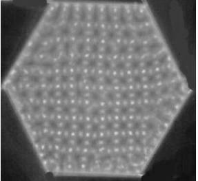
[0027] (d Discharge conditions: voltage frequency 53kHz, voltage amplitude 4.3kV, air gap pressure 0.5Pa, argon content in the mixed gas in the air gap is 90%, discharge produces plasma photonic crystals with three quadrilateral structures nested. figure 2 one Figure 5 A schematic diagram of a plasmonic photonic crystal with three nested quadrilateral structures produced in this example. Figure 4 Middle: A is the structure diagram of the plasma ph...
Embodiment 2
[0029] First three steps are identical with embodiment 1, (d) step discharge condition is: applied voltage U=4.3kV, frequency f=53kHz, air pressure p=0.5Pa, argon content χ (Ar) = 90%. The pattern photo of the resulting plasmonic photonic crystal with three nested quadrilateral structures is shown in Image 6 shown.
Embodiment 3
[0031] First three steps are identical with embodiment 1, (d) step discharge condition is: applied voltage U=5.2kV, frequency f=53kHz, air pressure p=0.5Pa, argon content χ (Ar) = 75%. The pattern photo of the resulting plasmonic photonic crystal with three nested quadrilateral structures is shown in Figure 7 shown.
PUM
 Abstract
Description
Claims
Application Information
 - R&D
- Intellectual Property
- Life Sciences
- Materials
- Tech Scout
- Unparalleled Data Quality
- Higher Quality Content
- 60% Fewer Hallucinations
Browse by: Latest US Patents, China's latest patents, Technical Efficacy Thesaurus, Application Domain, Technology Topic, Popular Technical Reports.
© 2025 PatSnap. All rights reserved.Legal|Privacy policy|Modern Slavery Act Transparency Statement|Sitemap|About US| Contact US: help@patsnap.com


