Phase change memory and preparation method thereof

A phase change memory and memory technology, which is applied in semiconductor devices, electric solid state devices, electrical components, etc., to achieve the effect of increasing current efficiency and reducing leakage current

Active Publication Date: 2012-07-04
SEMICONDUCTOR MANUFACTURING INTERNATIONAL (BEIJING) CORP
View PDF4 Cites 0 Cited by
  • Summary
  • Abstract
  • Description
  • Claims
  • Application Information

AI Technical Summary

Problems solved by technology

The vertical diodes in the prior art are silicon PN junction diodes, so it is inevitable that the carrier leakage current caused by the electric field will be generated at the PN junction

Method used


Image

  • Phase change memory and preparation method thereof
  • Phase change memory and preparation method thereof
  • Phase change memory and preparation method thereof

Examples


Embodiment Construction

[0068] In order to make the above objects, features and advantages of the present invention more comprehensible, specific implementations of the present invention will be described in detail below in conjunction with the accompanying drawings.

[0069] In the following description, many specific details are set forth in order to fully understand the present invention, but the present invention can also be implemented in other ways than those described here, so the present invention is not limited by the specific embodiments disclosed below.

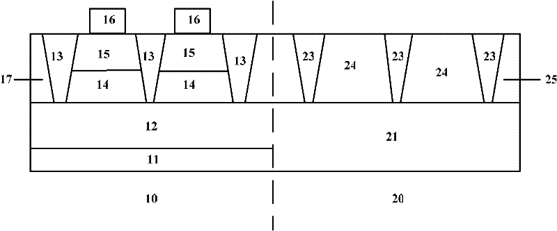
[0070] As mentioned in the background technology section, the peripheral circuit area cannot work well in the preparation of phase-change memory in the prior art, and the silicon PN junction diode will inevitably generate carrier leakage current caused by the electric field at the PN junction , which is not conducive to the realization of high density and low energy consumption of the phase change memory.

[0071] Therefore, in the prepar...


PUM

PropertyMeasurementUnit
Thicknessaaaaaaaaaa

Abstract

The invention relates to a phase change memory and a preparation method thereof, wherein the phase change memory comprises a peripheral circuit region and a memory region; a vertical diode in the memory region comprises an N-type conduction region and a P-type conduction region; the N-type conduction region is positioned above an N-type ion burial layer; the N-type ion burial layer is positioned on a memory substrate; a P-type substrate is positioned on the N-type conduction region; the upper surface of the P-type conduction region and the upper surface of a peripheral substrate of the peripheral circuit region are positioned on the same horizontal plane; a phase change layer is positioned on the P-type substrate; an MOS (metal oxide semiconductor) transistor is positioned on the peripheral substrate; and the P-type conduction region contains SiGe (silicon germanium). The preparation method comprises the following steps: firstly depositing a sacrifice dielectric layer on the peripheral substrate before preparing the vertical diode; then etching the memory substrate; and then removing the sacrifice dielectric layer after finishing preparation of the vertical diode; and finally preparing the phase change layer and the MOS transistor. According to the invention, the leakage current of the vertical diode is reduced, the current efficiency is improved, and the problem that the peripheral circuit region can not work well in the prior art is solved.

Description

technical field [0001] The invention relates to a device in the technical field of semiconductors and a preparation method thereof, in particular to a phase change memory and a preparation method thereof. Background technique [0002] Recently, a phase change random access memory (Phase Change RAM, PCRAM) device (phase change memory for short) has been proposed as a nonvolatile semiconductor memory device. A unit storage unit of a phase change memory uses a phase change material as a data storage medium. The phase change material has two stable phases (for example: amorphous phase and crystalline phase) according to the heat supplied to it. Known phase change materials include Ge—Sb—Te (GST) compound, which is a mixture of germanium (Ge), antimony (Sb), and tellurium (Te), among others. Heat is supplied to effect a phase change in the phase change material. [0003] If the phase change material is heated for a short time at a temperature close to its melting temperature a...

Claims


Application Information

Patent Timeline
IPC IPC(8): H01L45/00
CPCH01L45/144H01L45/06H01L27/24H01L27/15H01L45/00H01L45/1213H10N70/257H10N70/231H10N70/8828H10B63/10H10B63/00
Inventor 三重野文健何有丰
Owner SEMICONDUCTOR MANUFACTURING INTERNATIONAL (BEIJING) CORP
Why Eureka
Try Eureka