Backside electrode tape for thin film solar cell and method for manufacturing thin film solar cell
A technology of solar cells and back electrodes, which is applied in the direction of final product manufacturing, sustainable manufacturing/processing, circuits, etc., can solve the problems of increasing the number of manufacturing processes of thin-film solar cells, and achieve simplification of manufacturing processes, simple manufacturing, and manufacturing processes The effect of efficiency
- Summary
- Abstract
- Description
- Claims
- Application Information
AI Technical Summary
Problems solved by technology
Method used
Image
Examples
Embodiment 1
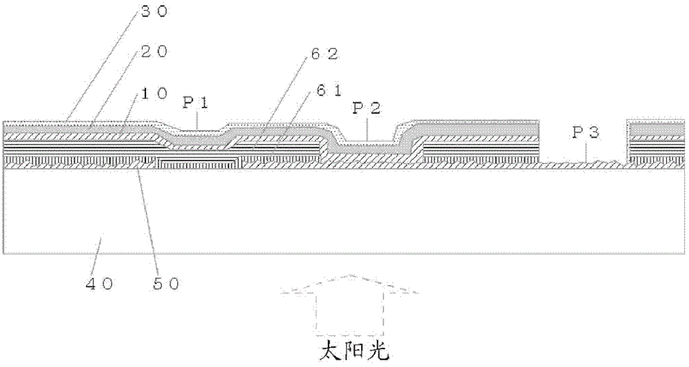
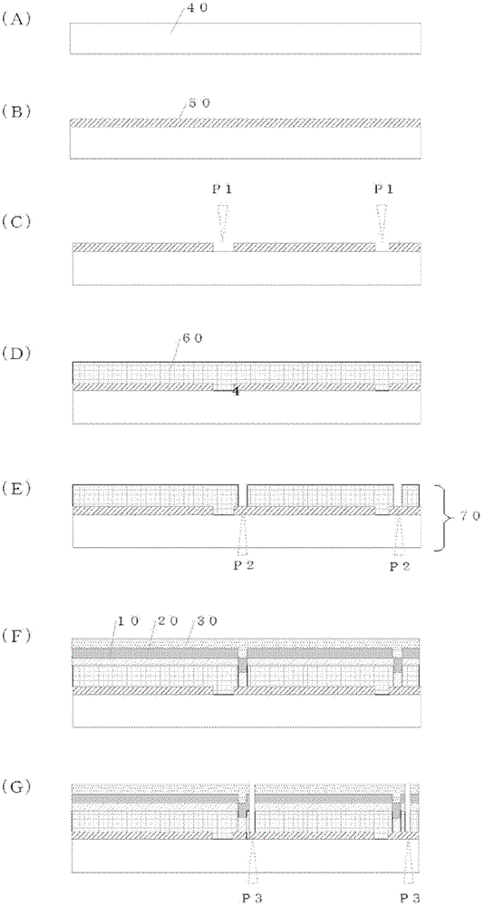
[0127] use figure 2 (A) to (E) explain the method of manufacturing the adherend, and the subsequent process uses Figure 5 Be explained. First, if figure 2 As shown in (B), the transparent substrate 40 is a glass plate with a length and width of 10 cm and a thickness of 4 mm, and SnO is used as the transparent conductive film 50. 2 . At this time, the film thickness of the transparent conductive film 50 is 800 nm, the sheet resistance is 10 Ω / □, and the haze is 15 to 20%.
[0128] Next, if figure 2 As shown in (C), an amorphous silicon layer 61 is formed with a thickness of 300 nm on the transparent conductive film 50 processed up to laser scribing P1 by plasma CVD, and then the amorphous silicon layer 61 is formed by plasma CVD. A microcrystalline silicon layer 62 is formed with a thickness of 1.7 μm, thereby forming a figure 2 The silicon-based photoelectric conversion layer 60 shown in (D). Such as figure 2 As shown in (E), the photoelectric conversion layer 60...
Embodiment 2~23
[0133] Except having set the conditions shown in Table 1, it tested by the method similar to Example 1. Here, as the silica sol-gel used in Example 2 and the like, SB-10A manufactured by Mitsubishi Material was used. And, the composition for reflective electrode thin films used by the wet coating method, such as Example 12, was produced as follows.
[0134]First, silver nitrate is dissolved in deionized water to prepare an aqueous solution of metal ions. Then, sodium citrate was dissolved in deionized water to prepare a sodium citrate aqueous solution having a concentration of 26% by mass. In the nitrogen gas flow maintained at 35°C, granular ferrous sulfate was directly added to the sodium citrate aqueous solution and dissolved to prepare a reducing agent aqueous solution containing citrate ions and ferrous ions in a molar ratio of 3:2. Next, in the state where the above-mentioned nitrogen gas flow is kept at 35° C., put the stirring bar of the magnetic stirrer into the red...
Embodiment 24
[0139] use Figure 5 Be explained. Figure 5 The adherend 7 shown in (a) used the adherend produced in Example 1. Next, silica sol-gel was coated as a barrier layer film 3a on a carrier tape 8a made of polyethylene terephthalate (PET) with a die coater so that the film thickness after heat treatment was 1 μm, and Heat treatment at 120°C for 10 minutes. On this basis, an Ag film of 800 nm was formed by sputtering as the reflective electrode thin film 2a.
[0140] Next, the composition for transparent electrode thin films used when forming the transparent electrode thin film 1a was prepared as follows. As conductive fine particles, 50 parts by mass of AZO powder having an atomic ratio of Al / (Al+Zn)=0.02 and a particle size of 0.03 μm was added, and IPA was added as a dispersion medium to make the whole 100 parts by mass. The mixture was run for 2 hours in a horizontal mill (horizontal bead mill) using zirconia beads with a diameter of 0.3 mm to disperse the fine particles in...
PUM
 Abstract
Description
Claims
Application Information
 - R&D
- Intellectual Property
- Life Sciences
- Materials
- Tech Scout
- Unparalleled Data Quality
- Higher Quality Content
- 60% Fewer Hallucinations
Browse by: Latest US Patents, China's latest patents, Technical Efficacy Thesaurus, Application Domain, Technology Topic, Popular Technical Reports.
© 2025 PatSnap. All rights reserved.Legal|Privacy policy|Modern Slavery Act Transparency Statement|Sitemap|About US| Contact US: help@patsnap.com


