Method for manufacturing one time programmable (OTP) device
A device manufacturing method and substrate technology, which are used in semiconductor/solid-state device manufacturing, electrical components, gaseous chemical plating, etc., can solve the problems of shortening the service life of OTP devices and increasing leakage current, and improve data storage characteristics and use. Longevity, the effect of avoiding the increase of defects
- Summary
- Abstract
- Description
- Claims
- Application Information
AI Technical Summary
Problems solved by technology
Method used
Image
Examples
Embodiment 1
[0037] As mentioned in the background section, the manufacturing process of the OTP device can be combined with the CMOS logic process (logic process), so that no additional mask layer is required. However, for 0.18μm embedded OTP devices, the problem of increased leakage current often occurs, which greatly shortens the service life of OTP devices.
[0038] The inventors have found that the reasons for the increase in the leakage current of the 0.18 μm embedded OTP device and the greatly shortened service life of the OTP device are:
[0039] In a common CMOS logic process, the function of the silicide barrier layer (Salicide Block, SAB) is to block part of the polysilicon and the substrate from surface metallization, so as to ensure sufficient resistance value to form the resistance part in the circuit. For embedded OTP devices, another function of the SAB layer is to cover the floating gate of the OTP device to protect the floating gate of the OTP device from being metallized...
Embodiment 2
[0049] The manufacturing method of the OTP device provided by the present invention will be described in detail below with a specific embodiment.
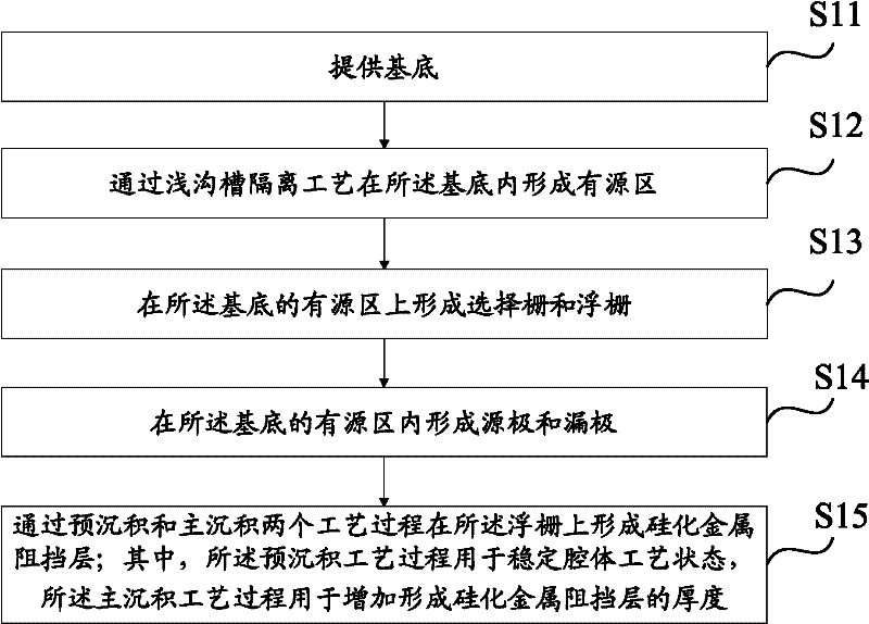
[0050] refer to figure 2 , figure 2 A schematic flow chart of another OTP device manufacturing method provided by the embodiment of the present invention, the method specifically includes the following steps:
[0051] Step S11: providing a substrate.
[0052] In this embodiment, the substrate is a P-type silicon substrate. In other embodiments, the substrate may also be a semiconductor material such as gallium arsenide, germanium, or silicon-on-insulator (SOI) or a combination of semiconductor materials.
[0053] Step S12: forming an active region in the substrate by shallow trench isolation process.
[0054] This step may further include the following steps:
[0055] Step S121 : forming shallow trenches in the substrate.
[0056] In this embodiment, the active regions are defined by a shallow trench isolation (STI) process,...
PUM
 Abstract
Description
Claims
Application Information
 - R&D
- Intellectual Property
- Life Sciences
- Materials
- Tech Scout
- Unparalleled Data Quality
- Higher Quality Content
- 60% Fewer Hallucinations
Browse by: Latest US Patents, China's latest patents, Technical Efficacy Thesaurus, Application Domain, Technology Topic, Popular Technical Reports.
© 2025 PatSnap. All rights reserved.Legal|Privacy policy|Modern Slavery Act Transparency Statement|Sitemap|About US| Contact US: help@patsnap.com


