LED light source using optical glass filter
A technology of LED light source and optical glass, which is applied in the field of light filtration, can solve the problems of no transparent substrate coating process, no band filter, etc., so as not to affect the visible light transmittance, high ultraviolet cut-off rate, and reduce the hazards of light radiation Effect
- Summary
- Abstract
- Description
- Claims
- Application Information
AI Technical Summary
Problems solved by technology
Method used
Image
Examples
Embodiment 1
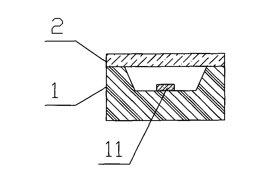
[0043] see figure 1 , an LED device 1, in which an LED chip 11 is encapsulated, and an optical glass filter 2 is located above the LED chip 11 and fixed.
[0044] When working, the light emitted by the LED chip 11 must pass through the optical filter 2 before it can be emitted to the outside. The optical filter 2 filters the light emitted by the LED chip within the range of wavelengths less than 445nm and greater than 700nm.
[0045] LED chip 11 can choose any desired emission wavelength, such as green light with a dominant wavelength of 530nm, or red light with a dominant wavelength of 620nm; another example is blue light with a dominant wavelength of 460nm, and mix a certain proportion in the potting glue YAG powder, the blue light emitted by the LED chip excites the YAG powder, and finally obtains white light with a color temperature of 8000K or other required color temperatures.
[0046] The preparation of the optical filter with dual functions of cutting off ultraviolet ...
Embodiment 2
[0058] It is basically the same as in Example 1, except that the preparation of the optical filter is performed by magnetron sputtering coating the inner film on the transparent substrate of optical glass with a silicon target and a tantalum pentoxide target. On this basis, the The product is obtained by magnetron sputtering coating the outer film from the titanium oxide-cerium oxide target.
Embodiment 3
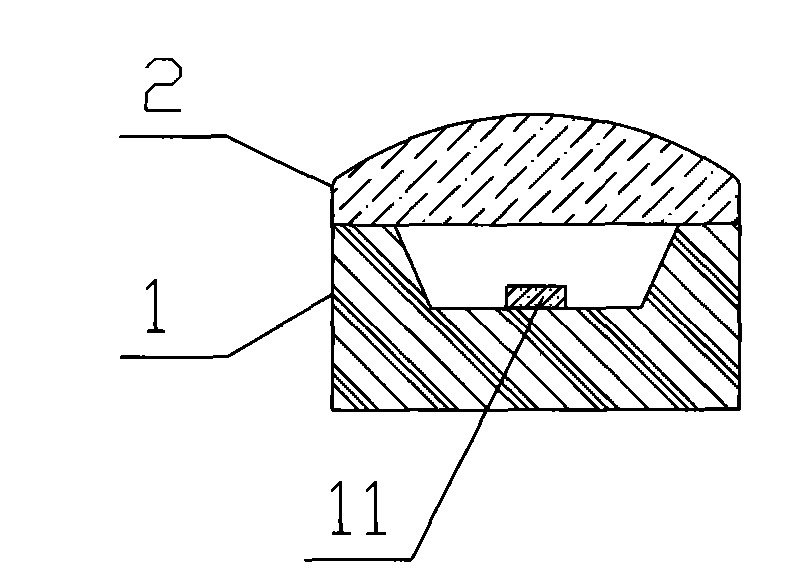
[0060] Basically the same as Embodiment 1, the difference is that the optical filter is formed into a circular lens surface by an optical glass transparent substrate, such as figure 2 shown; or shaped into a square lens surface, and then cleaned and coated.
PUM
| Property | Measurement | Unit |
|---|---|---|
| Thickness | aaaaa | aaaaa |
Abstract
Description
Claims
Application Information
 - Generate Ideas
- Intellectual Property
- Life Sciences
- Materials
- Tech Scout
- Unparalleled Data Quality
- Higher Quality Content
- 60% Fewer Hallucinations
Browse by: Latest US Patents, China's latest patents, Technical Efficacy Thesaurus, Application Domain, Technology Topic, Popular Technical Reports.
© 2025 PatSnap. All rights reserved.Legal|Privacy policy|Modern Slavery Act Transparency Statement|Sitemap|About US| Contact US: help@patsnap.com


