Microelectronic packages and associated methods of manufacturing

A technology of microelectronic packaging and manufacturing methods, which is applied in the direction of circuits, electrical components, and electrical solid devices, can solve the problems of solder ball collapse, difficult operation, time-consuming, etc., and achieve the effect of controlling collapse

Inactive Publication Date: 2012-06-27
CHENGDU MONOLITHIC POWER SYST
View PDF5 Cites 10 Cited by
  • Summary
  • Abstract
  • Description
  • Claims
  • Application Information

AI Technical Summary

Problems solved by technology

[0003] A disadvantage of the flip-chip technique described earlier is that when the substrate is a leadframe with multiple pins, the solder balls may collapse uncontrollably during reflow
Uncontrolled solder ball collapse can lead to structural, functional and / or other types of damage to microelectronic packages
For example, adjacent solder balls may contact each other, causing a short circuit in the semiconductor chip and / or substrate
[0004] The traditional solution is to make a solder mask on a lead frame similar to a printed circuit board, but making a solder mask on the tiny pins of a lead frame is difficult, time-consuming, and expensive

Method used


Image

  • Microelectronic packages and associated methods of manufacturing
  • Microelectronic packages and associated methods of manufacturing
  • Microelectronic packages and associated methods of manufacturing

Examples


Embodiment Construction

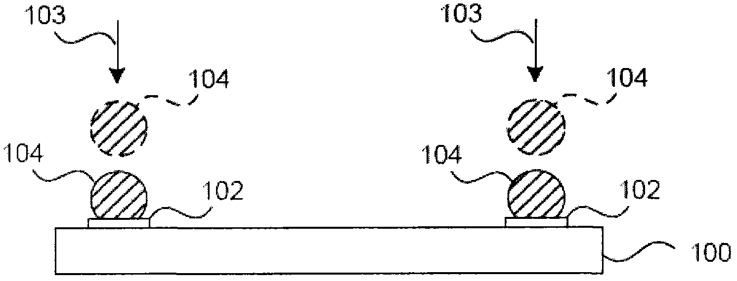
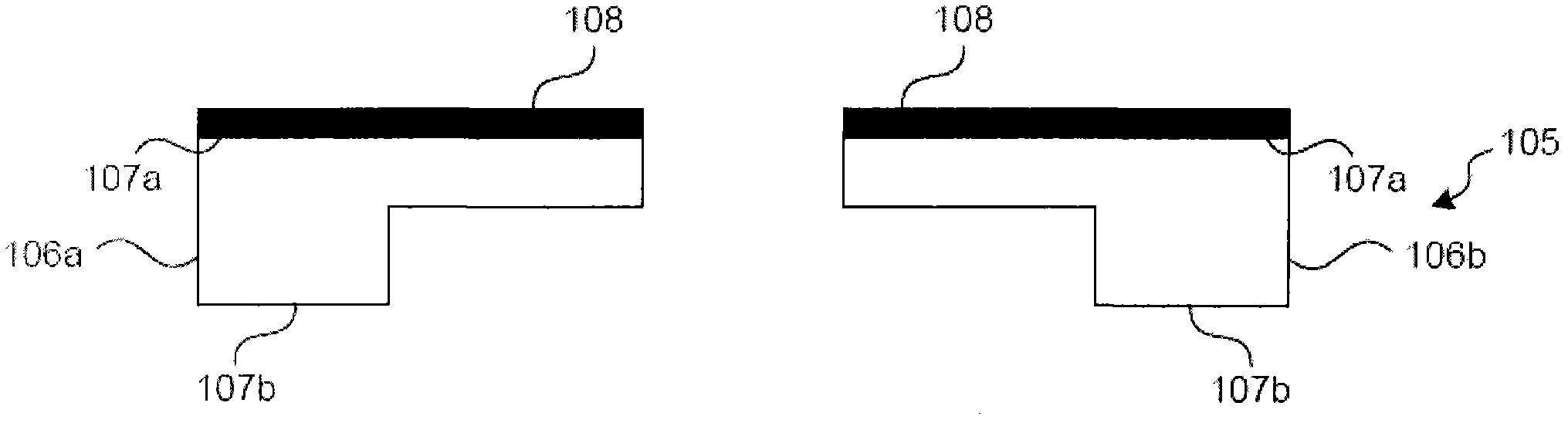
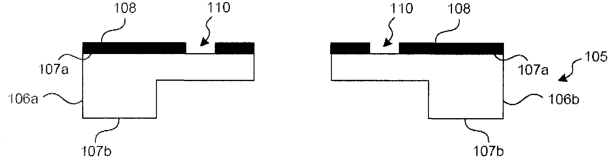
[0015] Embodiments of the present invention are described below with reference to the drawings. A package packaged with a semiconductor chip is called a microelectronic package. Usually, a microelectronic package provides protection, power supply, and cooling for the internal chip and related components while minimizing the impact on the electrical performance of the semiconductor chip, and provides electrical and external connections. and mechanical contact. A typical microelectronic package includes microelectronic circuits or components, thin film recording heads, data storage units, microfluidic devices, and other components formed on microelectronic substrates. Microelectronic substrates may include semiconductor substrates (such as wafers doped with silicon or gallium arsenide), insulating sheets (such as ceramic substrates), or conductive sheets (such as metals or metal alloys). The "semiconductor chip" referred to herein may include products used in various situations...


PUM


Abstract

The invention discloses microelectronic packages and associated methods of manufacturing. In one embodiment, a method of manufacturing the microelectronic packages includes forming an attachment area and a non-attachment area on a lead finger of a lead frame. The attachment area is more wettable to the solder ball than the non-attachment area during reflow. The method also includes contacting a solder ball carried by a semiconductor die with the attachment area of the lead finger, reflowing the solder ball while the solder ball is in contact with the attachment area of the lead finger, and controllably collapsing the solder ball to establish an electrical connection between the semiconductor die and the lead finger of the lead frame.

Description

technical field [0001] The invention relates to an electronic component, in particular to a microelectronic package and a manufacturing method thereof. Background technique [0002] Flip-chip technology is a technology that directly connects a semiconductor chip to a substrate through solder balls or solder bumps. In the packaging process, the solder balls are first placed on the semiconductor chip, and a solder mask is formed on the substrate (such as a printed circuit board) to determine multiple connection points, and then the semiconductor chip with the solder balls attached is turned over and the solder The balls are aligned to the corresponding connection points on the substrate, and the connections are finally reflowed. [0003] A disadvantage of the flip-chip technique described earlier is that when the substrate is a lead frame with multiple pins, the solder balls may collapse uncontrollably during reflow. Uncontrolled solder ball collapse may result in structural...

Claims


Application Information

Patent Timeline
Patent Type & Authority Applications(China)
IPC IPC(8): H01L21/48H01L21/60H01L23/495
CPCH01L2924/01082H01L2924/0105H01L2224/13118H01L2224/32245H01L2224/1146H01L24/13H01L2924/13091H01L2224/13116H01L23/49582H01L2924/01029H01L2224/13147H01L2224/11849H01L21/563H01L2224/81439H01L2224/16245H01L23/49548H01L2924/014H01L2224/81191H01L2924/3841H01L2924/0103H01L2224/831H01L2224/92125H01L2224/81455H01L24/81H01L2224/11334H01L2924/01047H01L2224/81447H01L2924/01079H01L2224/73204H01L2224/81444H01L2924/13062H01L2224/81815H01L2224/16258H01L2224/13139H01L2924/14H01L23/49572H01L2924/01033H01L2924/01005H01L24/11H01L2924/01006H01L23/3107H01L21/52H01L2224/131H01L24/16H01L2224/8121H01L2224/13111H01L2924/13055H01L2924/1306H01L2924/1305H01L2924/15787H01L2924/181H01L2924/12042H01L2924/00014H01L2924/00012H01L2924/00H01L21/76885H01L23/4951H01L23/49575H01L23/3157H01L23/4952H01L24/17
Inventor 蒋航
Owner CHENGDU MONOLITHIC POWER SYST
Why Eureka
Try Eureka