
Manufacturing method for indium tin oxide (ITO)/zinc sulfide (ZnS)/cadmium selenide (CdSe)/ZnS/aluminum (Al) structure with visible light and near-infrared luminescence emission characteristics

A technology of emission characteristics and manufacturing methods, applied in the direction of electrical components, circuits, semiconductor devices, etc., can solve the problems of device stability and life, and achieve the effects of wide emission wavelength range, low turn-on voltage, and simple manufacturing methods

Inactive Publication Date: 2012-06-20
ZHEJIANG UNIV
View PDF3 Cites 7 Cited by
  • Summary
  • Abstract
  • Description
  • Claims
  • Application Information

AI Technical Summary

Problems solved by technology

The use of organic materials makes the stability and lifetime of the device problematic

Method used


Image

  • Manufacturing method for indium tin oxide (ITO)/zinc sulfide (ZnS)/cadmium selenide (CdSe)/ZnS/aluminum (Al) structure with visible light and near-infrared luminescence emission characteristics
  • Manufacturing method for indium tin oxide (ITO)/zinc sulfide (ZnS)/cadmium selenide (CdSe)/ZnS/aluminum (Al) structure with visible light and near-infrared luminescence emission characteristics
  • Manufacturing method for indium tin oxide (ITO)/zinc sulfide (ZnS)/cadmium selenide (CdSe)/ZnS/aluminum (Al) structure with visible light and near-infrared luminescence emission characteristics

Examples


Embodiment Construction

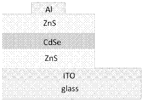
[0024] The technical scheme of the present invention is described in further detail below by specific embodiments:

[0025] (1) Preparation of ITO substrate.

[0026] The ITO substrate is purchased from the market, the thickness of ITO is 60nm, and it needs to be cleaned and degassed before growth.

[0027] (2) The first layer of ZnS film is grown by thermal evaporation.

[0028] The ZnS film was grown at room temperature with a thickness of 150nm and a growth pressure of 4×10 -3 Pa.

[0029] (3) Spin-coat CdSe quantum dots with a thickness of 500nm and allow them to air-dry naturally.

[0030] (4) The second layer of ZnS film is grown by thermal evaporation.

[0031] The ZnS film was grown at room temperature with a thickness of 150nm and a growth pressure of 4×10 -3 Pa.

[0032] (5) Thermal evaporation Al electrode.

[0033] A 200nm Al thin film was grown at room temperature as an electrode layer.

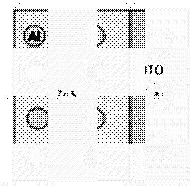
[0034] (6) Photolithography to form electroluminescent device patter...


PUM


Abstract

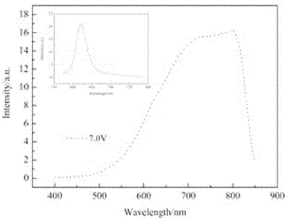
The invention provides a device structure and a manufacturing method thereof. The device structure is manufactured by utilizing quantum dots with a single dimension, emits light at a visible light waveband and a near-infrared waveband, and can generate laser. The manufacturing method comprises the following steps of: growing a zinc sulfide (ZnS) thin film on an indium zinc oxide (ITO) substrate; spin-coating cadmium selenide (CdSe) colloidal quantum dots on the ZnS thin film; growing another ZnS thin film and a metal electrode on the quantum dots; performing photoetching to form a device pattern; and performing packaging on the metal electrode to lead out a wire. The device structure has the light-emitting wavelengths of 450 to 850nm, and can emit visible light and near-infrared light on the basis of the surface defect state of the quantum dots, generate the laser by electrically exciting the population inversion of the energy level of the surface defect state, and be used for light-emitting diode (LED) white light illumination devices, laser devices and the like.

Description

technical field [0001] The patent of the present invention relates to a white light and near-infrared band electroluminescence and a quantum dot device structure capable of generating laser light and a manufacturing method thereof. Background technique [0002] Due to the quantum size effect, controlling the size of quantum dots can control the emission wavelength of quantum dots, and the light emitted by quantum dots has good monochromaticity, high quantum efficiency, and the emission wavelength can cover almost the entire visible light region, so it is expected to be widely used in flat panels. Display technology and solar cells. Since the 1990s, a lot of research has been done on quantum dot white light devices. In the past, the research on quantum dot white light devices was all quantum dot white light devices composed of organic materials or a mixture of organic materials and inorganic materials, or excited quantum dots with other fluorescent materials. Light up. The ...

Claims


Application Information

Patent Timeline
Patent Type & Authority Applications(China)
IPC IPC(8): H01L33/26H01L33/06H01L33/00
Inventor 吴惠桢楼腾刚胡炼
Owner ZHEJIANG UNIV
Learn More