Etching liquid for displaying void type defects of heavy-doped N-type Czochralski silicon single crystal
A technology of Czochralski silicon and etching solution, which is used in the preparation of test samples, optical test flaws/defects, etc., can solve problems such as unsuitable silicon single crystal, and achieve regular morphology, fast corrosion rate, and wide application range. Effect
- Summary
- Abstract
- Description
- Claims
- Application Information
AI Technical Summary
Problems solved by technology
Method used
Image
Examples
Embodiment 1
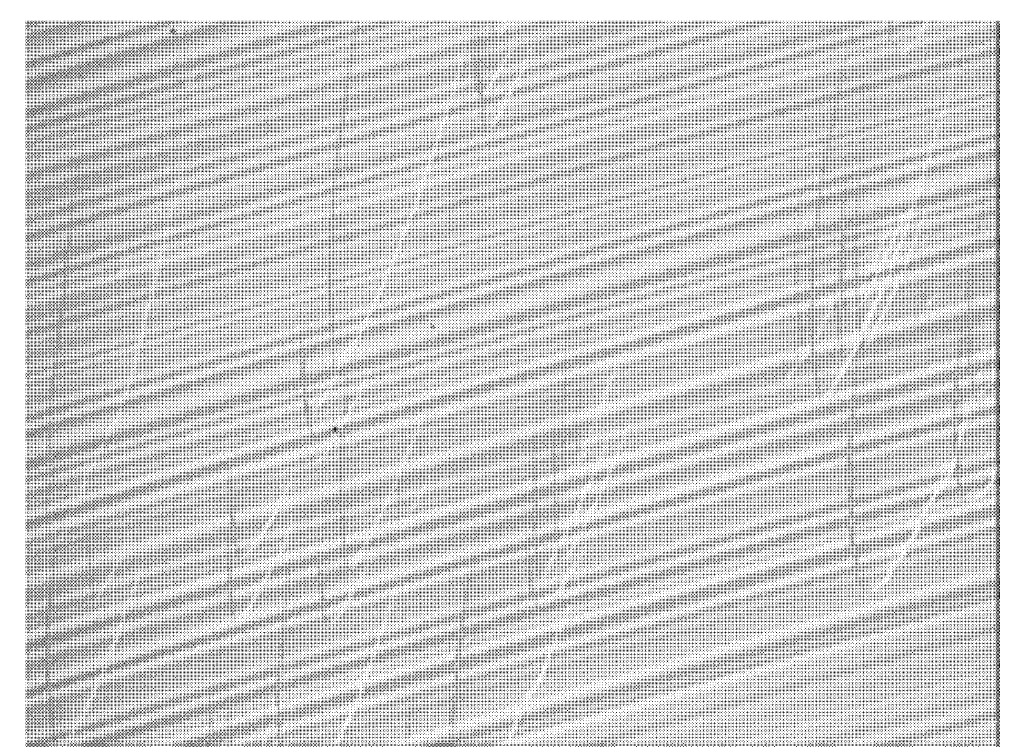
[0035] Example 1 Using an etchant to show void-type defects in a Czochralski silicon single crystal heavily doped with arsenic in the crystal orientation
[0036] The silicon wafer is a Czochralski silicon single crystal heavily doped with arsenic in the crystal direction, and its doping concentration is 1.6×10 19 cm -3 , the resistivity is 4.0mΩ·cm.
[0037] Preparation of corrosion solution: prepare chromium trioxide solution with a molar concentration of 0.2mol / L and hydrofluoric acid with a mass concentration of 40% respectively; according to the volume ratio of 1:1, use a graduated cylinder to measure hydrofluoric acid and add it to the chromium trioxide solution In, mix well.
[0038] Etching solution is used for the display of void-type defects on silicon wafers, and the specific steps include:
[0039] (1) Clean the silicon wafer with RCA standard cleaning solution;
[0040] (2) Put the beaker with the corrosive solution in a constant temperature water bath at 30...
Embodiment 2
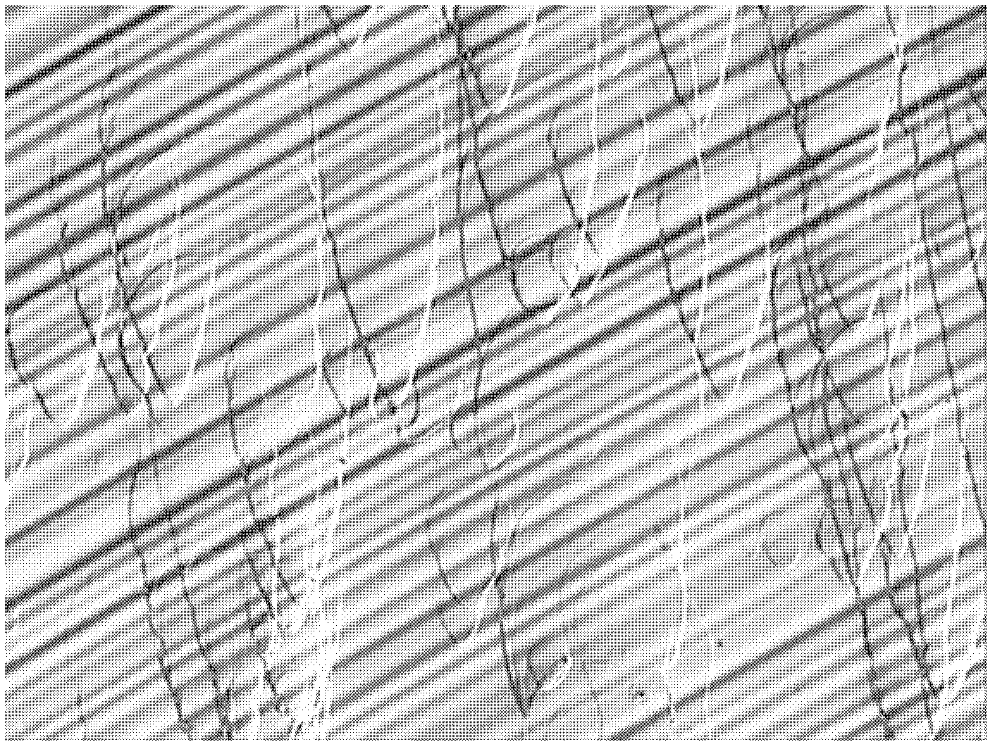
[0048] Example 2 Using Etching Solution to Display Cavity Defects in the Crystal Orientation Heavy Phosphorus-doped Czochralski Silicon Single Crystal
[0049] The silicon wafer is a Czochralski silicon single crystal heavily doped with phosphorus in the crystal direction, and its doping concentration is 7.4×10 19 cm -3 , the resistivity is 1.0mΩ·cm.
[0050] Preparation of corrosion solution: prepare chromium trioxide solution with a molar concentration of 0.2mol / L and hydrofluoric acid with a mass concentration of 40% respectively; according to the volume ratio of 1:1, use a graduated cylinder to measure hydrofluoric acid and add it to the chromium trioxide solution In, mix well.
[0051] The etchant is used for the display of void-type defects on silicon wafers. The specific steps are the same as those in Example 1. The defect morphology after being photographed by an optical microscope is shown in image 3 .
Embodiment 3
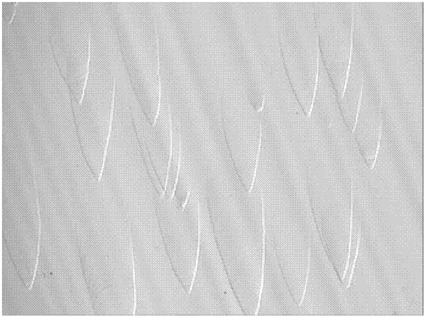
[0055] Example 3 Using Etching Solution to Display Cavity Type Defects in the Crystalline Heavily Doped Phosphorous Czochralski Silicon Single Crystal
[0056] The silicon wafer is a Czochralski silicon single crystal heavily doped with phosphorus in the crystal direction, and its doping concentration is 1.1×10 20 cm -3 , the resistivity is 0.7mΩ·cm.
[0057] Preparation of corrosion solution: prepare chromium trioxide solution with a molar concentration of 0.2mol / L and hydrofluoric acid with a mass concentration of 40% respectively; according to the volume ratio of 1:1, use a graduated cylinder to measure hydrofluoric acid and add it to the chromium trioxide solution In, mix well.
[0058] Etching solution is used for the display of void-type defects on silicon wafers, and the specific steps are the same as those in Example 1; Figure 5 .
[0059] Depend on Figure 5 It can be seen that after the silicon wafer is etched by this embodiment, the defects of the flow patte...
PUM
| Property | Measurement | Unit |
|---|---|---|
| electrical resistivity | aaaaa | aaaaa |
| electrical resistivity | aaaaa | aaaaa |
| electrical resistivity | aaaaa | aaaaa |
Abstract
Description
Claims
Application Information
 - R&D
- Intellectual Property
- Life Sciences
- Materials
- Tech Scout
- Unparalleled Data Quality
- Higher Quality Content
- 60% Fewer Hallucinations
Browse by: Latest US Patents, China's latest patents, Technical Efficacy Thesaurus, Application Domain, Technology Topic, Popular Technical Reports.
© 2025 PatSnap. All rights reserved.Legal|Privacy policy|Modern Slavery Act Transparency Statement|Sitemap|About US| Contact US: help@patsnap.com


