
Method for adjusting chip graph density using redundancy graph insertion,

A technology of graphic density and redundant graphics, which is applied in special data processing applications, instruments, electrical digital data processing, etc., can solve the problems of disregarding the graphic density value, high graphic density, and low graphic density, so as to avoid insufficient graphic density. Uniformity problem, effect of improving uniformity

Active Publication Date: 2012-05-23
SHANGHAI HUAHONG GRACE SEMICON MFG CORP
View PDF4 Cites 21 Cited by
  • Summary
  • Abstract
  • Description
  • Claims
  • Application Information

AI Technical Summary

Problems solved by technology

But the disadvantage may be that the area where the original graphics density is not high, after filling the virtual graphics around, the graphics density changes more
Insert redundant graphics for each area, but do not consider the graphic density value of the area around this area, only consider whether the graphic density of the current area meets the conditions, so the difference in graphic density in the local area may be will be big

Method used


Image

  • Method for adjusting chip graph density using redundancy graph insertion,
  • Method for adjusting chip graph density using redundancy graph insertion,
  • Method for adjusting chip graph density using redundancy graph insertion,

Examples


Embodiment Construction

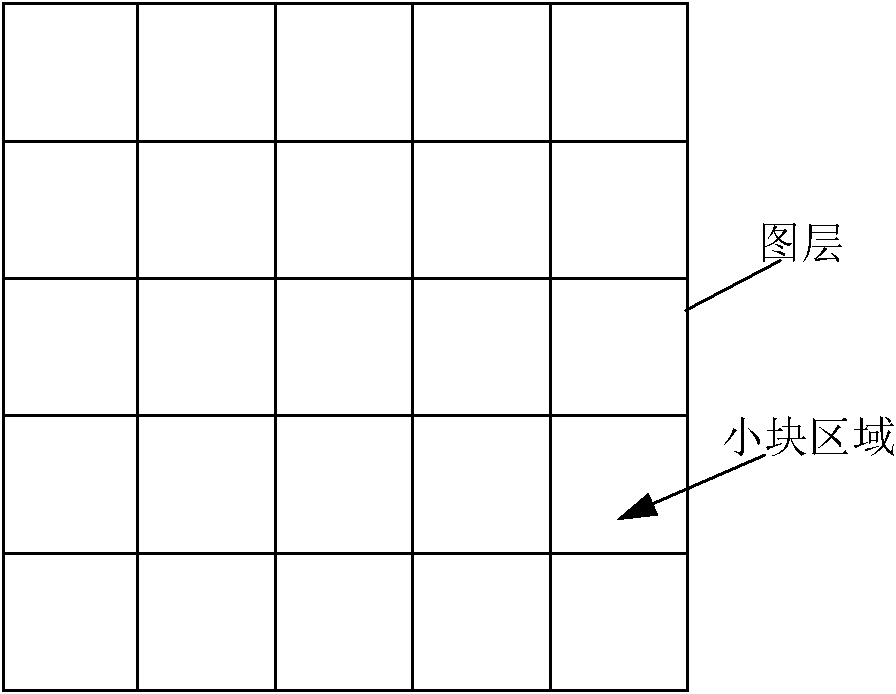
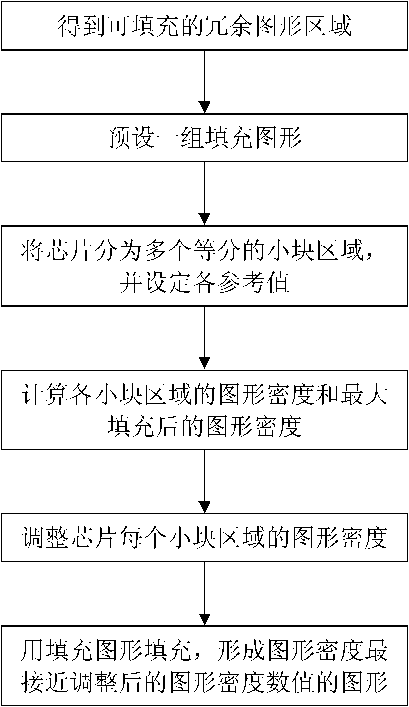
[0018] The method of the present invention is to design a filling pattern scheme with a predetermined pattern density for the layer that is about to carry out a CMP process or an etching process, then copy and make this design into the current layer, and then perform a CMP process or etching craft. The method for adjusting chip pattern density by utilizing redundant pattern filling of the present invention comprises the following steps (see figure 2 ):

[0019] (1) According to the filling rules, the fillable area of ​​a certain layer in the chip preparation (that is, the layer that needs to be filled with redundant graphics, such as the polysilicon layer) is obtained. Because the insertion of redundant graphics may affect the electrical performance of the chip, the fillable area is not equal to the blank area of ​​the current layer, and is usually smaller than the blank area of ​​the current layer. The filling rule is that the insertion of the filling pattern cannot affect...


PUM


Abstract

The invention discloses a method for adjusting graph density of a chip using redundancy graph filling, comprising the following steps: obtaining a fillable area in a certain graph layer of chip preparation; presetting a group of filling graphs with different graph densities; equivalently dividing into a plurality of small areas, and setting the graph density of the layer after filling, the minimal graph density value, the maximal graph density value of the small areas and the maximal graph density difference value between two adjacent small areas; calculating the initial graph density value of each small area; calculating the graph density value of the small area after filled with filling graph with maximal graph density; adjusting the graph density of each small area adopting virtual graph filling method; and filling the fillable areas of each small area to enable the graph density value of the filled small area to be close to the graph density value adjusted by Step (6). With the method, the uniformity of the graph densities of partial areas filled is improved.

Description

technical field [0001] The invention relates to a method for adjusting chip pattern density by using redundant pattern filling. Background technique [0002] With the continuous improvement of integrated circuit process technology, especially after the 0.13 micron process, the line width of the silicon process is already smaller than the wavelength length of exposure, making process stability more and more difficult. In the early stage of design, the derivation effect of the process is considered, resulting in many design for manufacturability (DFM, Design for Manufacturability) rules. For example, the uniformity of the pattern density (Pattern Density) in the silicon wafer is good, that is, the smaller the difference in the local pattern density, the smaller the impact on the macro load of chemical mechanical grinding and etching. [0003] It has a great influence on the chemical mechanical polishing (CMP, Chemical Mechanical Polarization) process and the macro loading (Ma...

Claims


Application Information

Patent Timeline
IPC IPC(8): H01L21/02G06F17/50H01L21/00
Inventor 陈福成
Owner SHANGHAI HUAHONG GRACE SEMICON MFG CORP
Learn More