Semiconductor refrigerating device

A refrigeration device and semiconductor technology, applied in the direction of semiconductor devices, semiconductor/solid-state device parts, electric solid-state devices, etc., can solve the problems of inability to conduct heat, low thermal conductivity, discounted cooling effect, etc., and achieve convenient use and small size. , the effect of high work efficiency

Inactive Publication Date: 2012-05-09
OCEANS KING LIGHTING SCI&TECH CO LTD +1
View PDF8 Cites 5 Cited by
  • Summary
  • Abstract
  • Description
  • Claims
  • Application Information

AI Technical Summary

Problems solved by technology

However, the existing semiconductor refrigerators mainly use two pieces of Al 2 o 3 The so-called sandwich structure in which the ceramic sheet sandwiches the p-type semiconductor and the n-type semiconductor, due to Al 2 o 3 The thermal conductivity of ceramics is not high, generally 20-30W / mK, which is far lower than that of some metals. For example, copper can reach 360W / mK, which is Al 2 o 3 nearly 18 times that of ceramics, so the use of Al 2 o 3 The ceramic semiconductor cooling chip cannot conduct heat quickly, which undoubtedly greatly reduces its cooling effect and is not conducive to heat dissipation

Method used


Image

  • Semiconductor refrigerating device
  • Semiconductor refrigerating device
  • Semiconductor refrigerating device

Examples


Embodiment 1

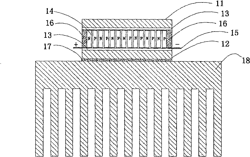
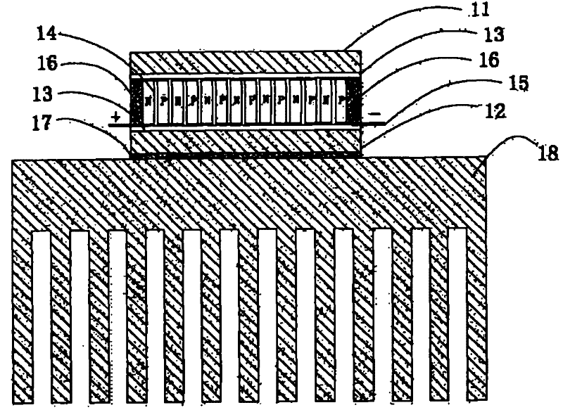
[0030] Such as figure 1 As shown, the semiconductor refrigeration device uses the cold end part 11 and the hot end part 12 of copper material with higher thermal conductivity and larger heat capacity, and the shape is a smooth and flat sheet, and the cold end part 11 and the heat One surface of the end part 12 is prepared by magnetron sputtering, chemical vapor deposition and other techniques to prepare a 50μm thick AlN thermally conductive insulating layer with high thermal conductivity; several p-type semiconductors 14 and n-type semiconductors 14 pass through the electrodes 15 are connected in series end to end, and the p-type semiconductor 14 and the n-type semiconductor 14 are spaced apart and arranged in parallel on the same plane; the cold end part 11 and the hot end part 12 are attached and connected to the p-type semiconductor 14 and the n-type semiconductor 14 ; Because AlN has a high thermal conductivity, up to 270W / mk, which can quickly conduct heat away, the AlN the...

Embodiment 2

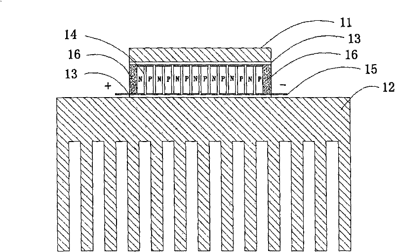
[0033] Such as figure 2 As shown, the structure of the semiconductor refrigeration device in this embodiment is similar to that of Embodiment 1, except that the hot end part 12 is made into a block with a fin tail, and at the same time, the heat sink 18 and thermally conductive silica gel are omitted. 17; Compared with Example 1, the heat sink 18 is omitted, which makes the heat dissipate faster and reduces the use of thermally conductive silicone grease, that is, reduces the thermal resistance in the thermal channel, and can better improve the heat dissipation rate ; At the same time, it saves production costs.


PUM

PropertyMeasurementUnit
Thicknessaaaaaaaaaa

Abstract

The invention belongs to the field of refrigerating equipment, and discloses a semiconductor refrigerating device. The device comprises a plurality of n-type semiconductor chips and p-type semiconductor chips which are connected end to end in series through electrodes and arranged at intervals and in parallel on the same plane; two sides of a plane formed by the n-type semiconductor chips and the p-type semiconductor chips connected in series are respectively jointed through a cold end component and a hot end component; a heat insulation material is encapsulated in a peripheral clearance formed by the cold end component, the hot end component, the n-type semiconductor chips and the p-type semiconductor chips; and a heat conducting insulation layer is respectively arranged on the jointed contact faces of the hot end component, the hot end component, the n-type semiconductor chips and the p-type semiconductor chips. By using the semiconductor material with thermoelectric energy conversion property, the device has refrigerating function during electrifying, actively and quickly absorbs a large amount of heat generated when a heating electronic component works, and provides an efficient heat dissipation channel between the heating electronic component and radiating fins.

Description

Technical field [0001] The present invention relates to a refrigeration device, in particular to a semiconductor refrigeration device that is well suited for cooling heat-generating electronic components such as integrated circuit chips, power-type light emitting diodes (LEDs) and the like. Background technique [0002] Integrated circuit chips, LEDs (light-emitting diodes), etc. are all electronic components that generate high heat. If heat is concentrated, improper heat dissipation treatment may cause these electronic components to fail to work properly or even burn out. [0003] At present, the heat dissipation measures for these electronic components are mainly heat sinks or heat sinks + fans. There are many shortcomings to using heat sinks alone. One is that it requires a large area and a large space, and the other is heat return; The way to add a fan to assist the heat dissipation, including many mechanical parts used to drive the fan, any failure of these parts may cause the...

Claims


Application Information

Patent Timeline
IPC IPC(8): H01L23/38H01L23/36
Inventor 周明杰马文波陈贵堂
Owner OCEANS KING LIGHTING SCI&TECH CO LTD
Why Eureka
Try Eureka