Method for forming side wall and storage unit formed thereby

A technology of side walls and right-angled triangles, applied in the fields of electrical components, semiconductor/solid-state device manufacturing, circuits, etc., can solve problems such as difficulty in controlling device threshold voltage, reducing device performance, and short-channel effect of devices, so as to improve writing speed , device performance maintenance, and the effect of increasing the substrate current

Active Publication Date: 2014-02-05
SHANGHAI HUALI MICROELECTRONICS CORP
View PDF7 Cites 0 Cited by
  • Summary
  • Abstract
  • Description
  • Claims
  • Application Information

AI Technical Summary

Problems solved by technology

However, simply reducing the sidewall width will cause serious short channel effect (Short Channel Effect, SCE) of the device, making it difficult to control the threshold voltage of the device and reducing the performance of the device

Method used


Image

  • Method for forming side wall and storage unit formed thereby

Examples


Embodiment Construction

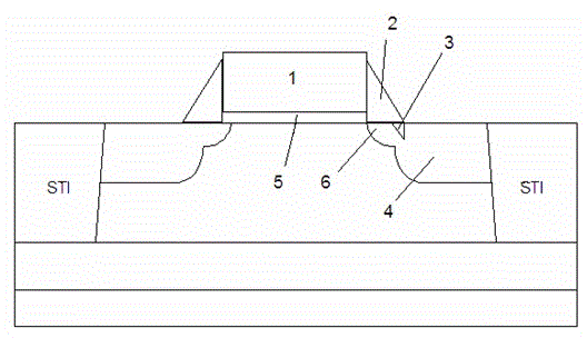
[0019] The present invention provides a method for forming sidewall spacers. The method includes: forming sidewall spacers of the gate structure on a semiconductor substrate having a gate structure and source / drain prefabricated regions; etching the formed sidewall spacers, Forming lower wide and upper narrow sidewalls; heavily doping the source and drain prefabricated regions with predetermined ions to form source and drain regions, and the predetermined ions used for heavily doping penetrate into the bottom of the sidewalls.

[0020] In the present invention, after the usual side wall etching process, an etching process for modifying the side wall profile is added, and the improved side wall profile is formed to form a right-angled triangular side wall. When the source and drain are heavily doped and implanted, some ions with higher energy will pass through the thinner sidewall regions and be implanted into the substrate. The implantation depth of this part of the ions is relat...


PUM


Abstract

The invention provides a method for forming a side wall. The method comprises the following steps of: forming the side wall of a gate structure on a semiconductor substrate having the gate structure and a source drain pre-preparation area; etching the formed side wall to form below wide on narrow shape side wall; and heavy doping the source drain pre-preparation area by predetermined ions to form a source drain area and so that the predetermined ions for heavy doping are permeated to the bottom of the side wall. When the method provided by the invention is used in the side wall etching process, the distribution of source drain heavy doping injection ions is adjusted by adjusting appearance of the etched side wall, therefore, the longitudinal electric field in a drain terminal channel can be improved, the substrate current is increased, the writing speed of a floating body effect storage unit is improved, and serious short-channel effect can not be generated so that the performance of devices can be kept.

Description

Technical field [0001] The present invention relates to the field of semiconductor preparation, in particular to an etching process for forming sidewalls, and the structure of a floating body effect memory cell (Floating Body Cell, FBC) formed by the method. Background technique [0002] The development of embedded dynamic storage technology has made large-capacity DRAM very popular in the current system-on-chip (SOC). The large-capacity embedded dynamic memory (eDRAM) brings various benefits to the SOC, such as improved bandwidth and reduced power consumption, which can only be realized through the use of embedded technology. In addition to transistors, each memory cell of the traditional embedded dynamic memory (eDRAM) also requires a deep trench capacitor structure. The deep trench of the capacitor makes the height of the memory cell much larger than its width, which makes the manufacturing process difficult. Its manufacturing process is very incompatible with the CMOS VLSI p...

Claims


Application Information

Patent Timeline
Patent Type & Authority Patents(China)
IPC IPC(8): H01L21/311H01L29/78
Inventor 俞柳江李全波
Owner SHANGHAI HUALI MICROELECTRONICS CORP
Why Eureka
Try Eureka