A Tunneling Field Effect Transistor with Increased On-state Current
A tunneling field effect, on-state current technology, applied in circuits, diodes, electrical components, etc., can solve problems such as difficult process realization, large off-state current of devices, and weak gate voltage control of the drain region. On-off ratio, low off-state current, and the effect of reducing process difficulty
- Summary
- Abstract
- Description
- Claims
- Application Information
AI Technical Summary
Problems solved by technology
Method used
Image

Examples
Embodiment 1
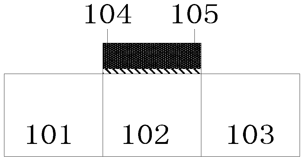
[0040] This embodiment is aimed at Figure 5 The Tunneling Field Effect Transistor (TFET) device that increases the on-state current is shown as an example of making an N-type TFET device. The polarized tunneling region is located in the P-type source region and is in contact with the epitaxial intrinsic region of the top layer. The length of the polarization tunneling region is the same as that of the gate, all of which are located under the gate.
[0041] The tunneling field effect transistor described in Embodiment 1 includes a source region 501 , an intermediate intrinsic region 502 , a drain region 503 , a polarization tunneling region 504 , an epitaxial intrinsic region 505 , sidewalls 506 , a gate oxide layer 507 , and a gate 508 . First, the source region, the middle intrinsic region, and the drain region are all made of silicon material to ensure that the source region can cause the polarization effect of the polarized tunneling region; secondly, ion implantation is p...
Embodiment 2
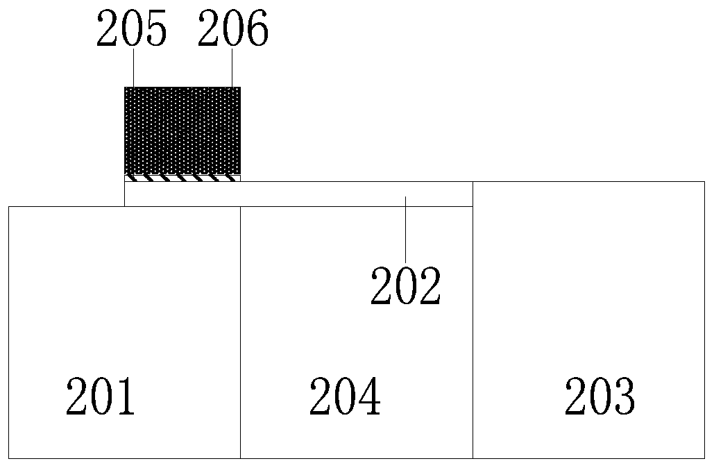
[0044] This embodiment is aimed at Figure 6 In the shown lateral tunneling field effect transistor (TFET) device for improving on-state current, its polarized tunneling region is located in the P-type source region and is in contact with the middle intrinsic region, and its upper surface coincides with the upper surface of the source region.
[0045] The tunneling field effect transistor described in Embodiment 2 includes a source region 601 , a polarized tunneling region 602 , an intermediate intrinsic region 603 , a drain region 604 , sidewalls 605 , a gate oxide layer 606 , and a gate 607 . First, the silicon material is still used to form the source region, the middle intrinsic region, and the drain region to ensure that the source region can cause the polarization effect of the polarized tunneling region, and the potential barrier of the middle intrinsic region can suppress the drift and diffusion of carriers; then Ion implantation is performed on the source region, the ...
Embodiment 3
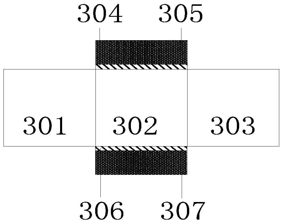
[0048] This embodiment is aimed at Figure 7 In the shown tunneling field effect transistor (TFET) device with an oxide layer, an oxide layer is set between the middle intrinsic region and the drain region of the device to realize dielectric isolation.
[0049] The tunneling field effect transistor described in Embodiment 3 includes a source region 701, an intermediate intrinsic region 702, a drain region 703, a polarization tunneling region 704, an epitaxial intrinsic region 705, sidewalls 706, a gate oxide layer 707, a gate 708, oxide layer 709 . First, the source region, the middle intrinsic region, and the drain region are all made of silicon material to ensure that the source region can cause the polarization effect of the polarized tunneling region; secondly, oxidation is carried out between the middle intrinsic region and the drain region to form an oxide layer 709; after that, ion implantation is performed on the source region, the middle intrinsic region and the drai...
PUM
 Abstract
Description
Claims
Application Information
 - R&D
- Intellectual Property
- Life Sciences
- Materials
- Tech Scout
- Unparalleled Data Quality
- Higher Quality Content
- 60% Fewer Hallucinations
Browse by: Latest US Patents, China's latest patents, Technical Efficacy Thesaurus, Application Domain, Technology Topic, Popular Technical Reports.
© 2025 PatSnap. All rights reserved.Legal|Privacy policy|Modern Slavery Act Transparency Statement|Sitemap|About US| Contact US: help@patsnap.com