
Three-dimensional measurement chip and system based on double-array image sensor

An image sensor and three-dimensional measurement technology, applied in image communication, TV system components, color TV components, etc., can solve the problems of complex system calibration, large number of hardware, poor registration accuracy, etc., and improve real-time performance , reduce computational stress, and eliminate calibration issues

Inactive Publication Date: 2012-05-02
TIANJIN UNIV
View PDF5 Cites 23 Cited by
  • Summary
  • Abstract
  • Description
  • Claims
  • Application Information

AI Technical Summary

Problems solved by technology

[0026] The purpose of the present invention is to solve the shortcomings of current 3D imaging methods and systems, such as the slow speed of obtaining depth information, poor registration accuracy between depth images and 2D images, a large number of hardware required by the entire 3D imaging system, and complicated system calibration. A dual image sensor array chip for stereo measurement for fast and high-precision acquisition of 3D images

Method used


Image

  • Three-dimensional measurement chip and system based on double-array image sensor
  • Three-dimensional measurement chip and system based on double-array image sensor
  • Three-dimensional measurement chip and system based on double-array image sensor

Examples


Embodiment Construction

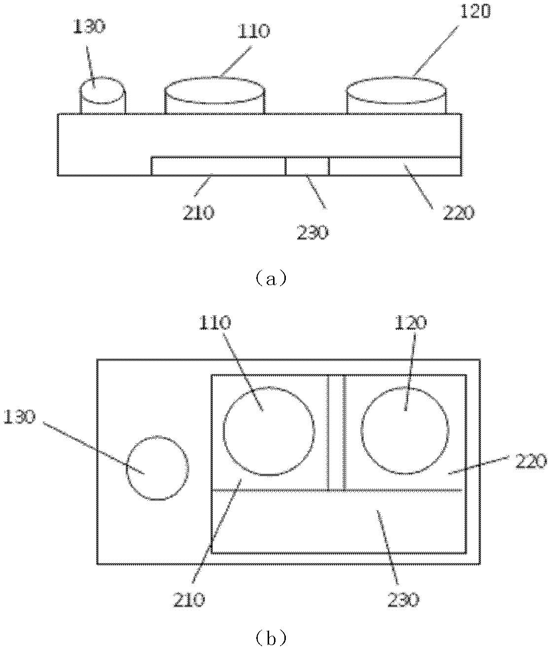
[0036] The present invention proposes to fabricate two image sensor arrays on one semiconductor substrate, which are located on the left and right sides of the semiconductor substrate respectively. An image sensor control circuit, an image signal processing circuit (ISP) and a digital signal processing circuit (DSP, mainly used to calculate depth information) are fabricated in the middle and below the two image sensor arrays, and the left and right image sensor arrays are connected through a bus. Apply wafer-level lens (Wafer Level Lens) technology to place optical lenses on two image sensor arrays. The two image sensor arrays work in different working modes: one as an ordinary image sensor array directly perceives ordinary two-dimensional image data; The target object is illuminated, whereby the image sensor array senses the infrared image data. The two image sensor arrays capture the image data and transmit the image data to the image signal processing circuit and the digit...


PUM


Abstract

The invention relates to the field of distance imaging and three-dimensional imaging technology, in particular to a three-dimensional measurement chip based on a double-array image sensor. The three-dimensional measurement chip comprises two optical lenses, two CMOS (complementary metal oxide semiconductor) image sensor arrays and an image sensor control and processing circuit, wherein the two CMOS image sensor arrays and the image sensor control and processing circuit are made on the same semiconductor substrate; the optical lenses are wafer-level optical lenses which are arranged on the two CMOS image sensor arrays respectively; one of the two optical lenses is provided with an infrared filter or film and used for obtaining a common two-dimensional color image, and the other optical lens is used for obtaining a range image; and the image sensor control and processing circuit establishes a three-dimensional image according to the image information obtained by the two CMOS image sensor arrays. The invention also provides a three-dimensional measurement system based on the chip. According to the invention, the size of the measurement chip and the system can be effectively reduced, and the real-time property and accuracy of the measurement are improved.

Description

technical field [0001] The present invention relates to the technical fields of distance imaging and three-dimensional imaging, and more specifically, relates to a three-dimensional measurement chip for obtaining stereoscopic image data. The chip integrates two CMOS optical sensor arrays, one for obtaining depth images and one for obtaining ordinary Two-dimensional image, by obtaining two kinds of information at the same time, to construct a three-dimensional image. Background technique [0002] CMOS chip [0003] The CMOS process is the mainstream process of VLSI, with a high degree of integration, and can integrate multiple functions on one chip according to needs. The CMOS image sensor chip adopts the CMOS process, and the image acquisition unit and the signal processing unit can be integrated on the same chip. The internal structure of the CMOS chip is mainly composed of photosensitive array, frame (row) control circuit and timing circuit, analog signal readout circuit...

Claims


Application Information

Patent Timeline
Patent Type & Authority Applications(China)
IPC IPC(8): H04N5/374H04N5/3745H04N5/378
Inventor 刘立倪海日王建王天慧
Owner TIANJIN UNIV
Learn More