Preparation method of metal-oxide-semiconductor field-effect transistor with silicon-on-nothing (SON) structure
A gate area and active area technology, applied in the field of MOSFET manufacturing process and field effect transistor manufacturing process, can solve the problems of complex process, affecting yield and high cost, achieving simple process, saving production cost and improving yield Effect
- Summary
- Abstract
- Description
- Claims
- Application Information
AI Technical Summary
Problems solved by technology
Method used
Image
Examples
Embodiment Construction
[0017] The device structure of the present invention will be further described below in conjunction with the accompanying drawings, which are not drawn to scale for the convenience of illustration.
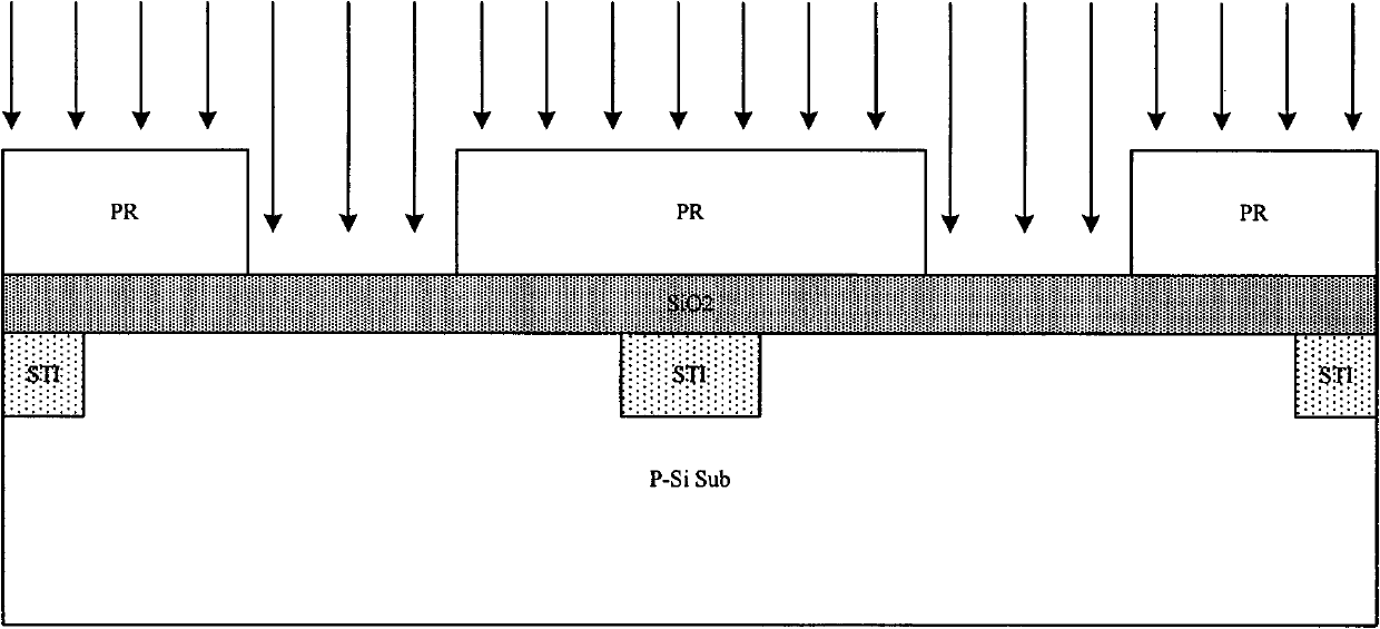
[0018] Please see Figure 1-4 , using the preparation method of the present invention, taking a CMOS device as an example, comprises the following steps:
[0019] Step one, such as figure 1 As shown, the active region is formed on the bulk silicon substrate (p-type Si substrate) by shallow trench isolation technology, which is exactly the same as the traditional bulk silicon CMOS process.
[0020] Step 2, forming a layer with a thickness of Above SiO 2 The buffer layer.
[0021] Step three, such as figure 2 As shown, using a photolithography plate for the gate region, the photoresist with the opposite polarity to the photoresist used in the photolithography process for the gate region is used for photolithography, so that the position for forming the gate region on the acti...
PUM
 Abstract
Description
Claims
Application Information
 - Generate Ideas
- Intellectual Property
- Life Sciences
- Materials
- Tech Scout
- Unparalleled Data Quality
- Higher Quality Content
- 60% Fewer Hallucinations
Browse by: Latest US Patents, China's latest patents, Technical Efficacy Thesaurus, Application Domain, Technology Topic, Popular Technical Reports.
© 2025 PatSnap. All rights reserved.Legal|Privacy policy|Modern Slavery Act Transparency Statement|Sitemap|About US| Contact US: help@patsnap.com


