Flash memory cell and method of forming same

A flash memory unit, p-type technology, applied in the direction of electrical components, electric solid-state devices, circuits, etc., can solve the problem of unstable storage performance of flash memory unit, and achieve the effect of improving reliability

Active Publication Date: 2016-02-03
SHANGHAI HUAHONG GRACE SEMICON MFG CORP
View PDF7 Cites 0 Cited by
  • Summary
  • Abstract
  • Description
  • Claims
  • Application Information

AI Technical Summary

Problems solved by technology

[0006] The problem solved by the present invention is to provide a flash memory unit and its forming method to solve the problem of unstable storage performance of the existing flash memory unit

Method used


Image

  • Flash memory cell and method of forming same
  • Flash memory cell and method of forming same
  • Flash memory cell and method of forming same

Examples


Embodiment Construction

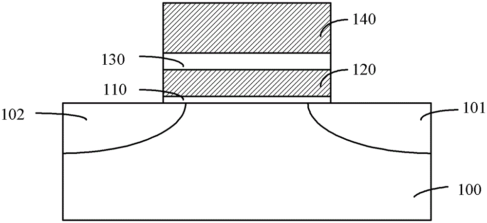
[0034] It can be known from the background art that the storage performance of the existing flash memory unit will decrease after being programmed many times.

[0035] The inventors conducted research on the above problems and found that when programming the existing flash memory cells, under the joint action of the drain voltage applied to the drain and the gate voltage applied to the control gate, hot electrons flow from the source to the control gate. The drain migrates and is implanted into the floating gate through the tunnel oxide as it moves. In the process of injecting hot electrons into the floating gate, most of the hot electrons cross to the floating gate from the part of the tunnel oxide layer close to the drain or facing the drain, and the hot electrons are easy to be damaged during multiple programming operations. The part of the tunnel oxide layer close to the drain or facing the drain causes damage, such as stress effects and trap charges; in subsequent program...


PUM


Abstract

The embodiment of the invention provides a flash memory unit and a forming method thereof. The flash memory unit disclosed by the embodiment of the invention comprises a semiconductor substrate, a gate structure positioned on the surface of the semiconductor substrate, and a source electrode and a drain electrode, wherein the gate structure comprises a tunneling oxide layer, a floating gate, an isolating oxide layer and a control gate which are sequentially formed; the source electrode and the drain electrode are positioned in the semiconductor substrates on two sides of the gate structure; the floating gate is provided with a first p-type doping end close to the drain electrode and a second p-type doping end close to the source electrode; and doping types of other parts are respectively in an n type. According to the flash memory unit and the forming method thereof disclosed by the invention, the memory property of the flash memory unit can be improved.

Description

technical field [0001] The invention relates to a semiconductor device and its forming method, in particular to a flash memory unit and its forming method. Background technique [0002] In the current semiconductor industry, integrated circuit products can be mainly divided into three types: analog circuits, digital circuits and digital / analog hybrid circuits, among which storage devices are an important type of digital circuits. In recent years, among storage devices, flash memory (flash memory, flash memory unit for short) has developed particularly rapidly. The main feature of the flash memory unit is that it can keep the stored information for a long time without power on; and it has the advantages of high integration, fast access speed, easy erasing and rewriting, etc. Has been widely used. [0003] The structure of the flash memory cell is different from that of conventional MOS transistors. The gate (gate) of a conventional MOS transistor and the conductive channel...

Claims


Application Information

Patent Timeline
Patent Type & Authority Patents(China)
IPC IPC(8): H01L27/115H01L21/8247H01L21/265
Inventor 曹子贵
Owner SHANGHAI HUAHONG GRACE SEMICON MFG CORP
Why Eureka
Try Eureka