Multi-source integrated color-adjustable light-emitting component and preparation method thereof
A technology of light-emitting components and colors, applied in electrical components, semiconductor devices, circuits, etc., can solve the problems of difficult to achieve ideal effect of light color mixing, uncontrollable color purity, and shortened LED life.
- Summary
- Abstract
- Description
- Claims
- Application Information
AI Technical Summary
Problems solved by technology
Method used
Image
Examples
Embodiment 1
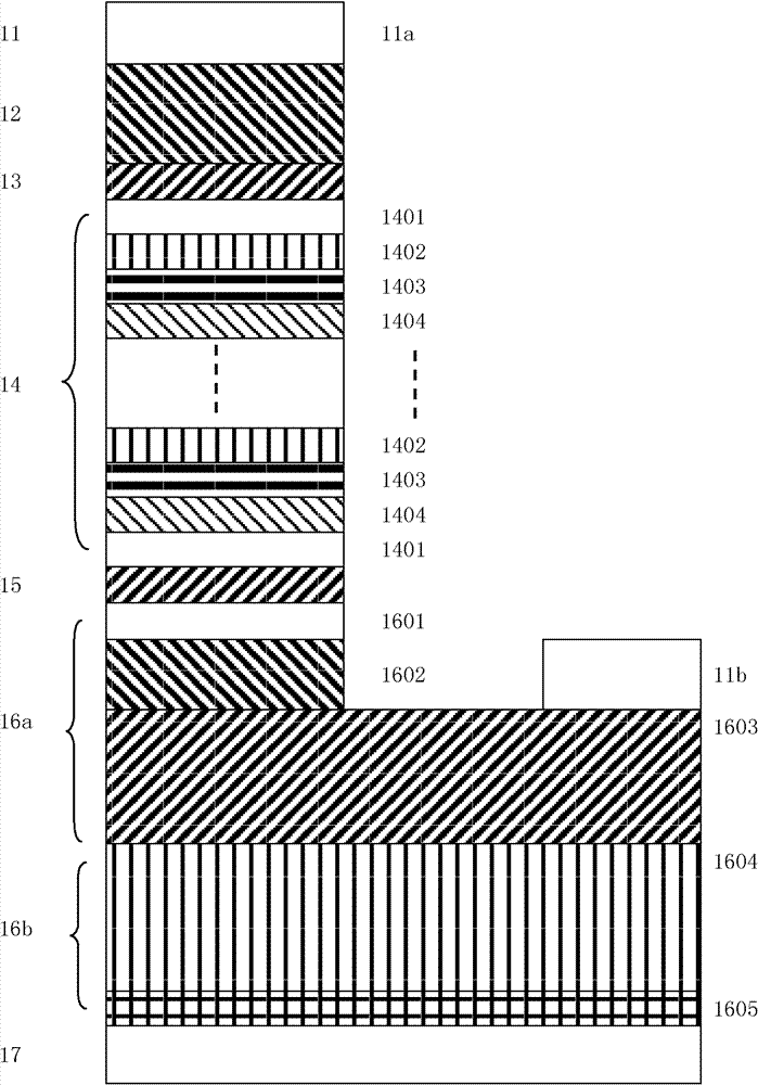
[0070] Red, green and blue three-color integrated and adjustable gallium nitride (GaN)-based light-emitting element, the structural diagram of the single-wavelength light-emitting part can be found in figure 1 , including from bottom to top:
[0071] (1) Substrate 17
[0072] A transparent growth substrate 17, the material of which can be sapphire;
[0073] (2) Buffer layer 16b
[0074] Close to the side of the substrate 17 is a layer of about 1000nm GaN buffer layer 16b, which can be n-type doped or not mixed according to the chip structure. GaN layer 1604 for reducing lattice mismatch;
[0075] (3) n-type semiconductor contact layer 16a
[0076] On the buffer layer 16b is an n-type semiconductor contact layer 16a of about 2000nm GaN material, which includes: a 500nm n-type GaN alignment layer 1602, the present embodiment adopts 500nm GaN:Si, n≥5×10 18 cm -3 , for etching into an array of quantum dot positioning holes; a 40nm n-type GaN improvement layer 1601 is deposit...
Embodiment 2
[0119] Red, green and blue three-color integrated and adjustable gallium nitride (GaN)-based light-emitting element, the structural diagram of the single-wavelength light-emitting part can be found in Figure 5 , including from bottom to top:
[0120] (1) substrate 57;
[0121] (2) buffer layer 56b;
[0122] (3) n-type semiconductor contact layer 56a;
[0123] (4) n-type semiconductor barrier layer 55;
[0124] (5) active layer 54;
[0125] (6) p-type semiconductor barrier layer 53;
[0126] (7) p-type semiconductor contact layer 52;
[0127] (8) Electrode layer 51 .
[0128] The difference between the single emission wavelength structure of this embodiment and the first embodiment lies in the active layer. Its active layer 54 uses mixed quantum dots and quantum wells as the main light-emitting structure, and at least includes from bottom to top:
[0129] 5-20nm GaN lower layer semiconductor pad layer 5401; its energy gap is larger than the quantum dot layer 5407, but sm...
PUM
 Abstract
Description
Claims
Application Information
 - R&D Engineer
- R&D Manager
- IP Professional
- Industry Leading Data Capabilities
- Powerful AI technology
- Patent DNA Extraction
Browse by: Latest US Patents, China's latest patents, Technical Efficacy Thesaurus, Application Domain, Technology Topic, Popular Technical Reports.
© 2024 PatSnap. All rights reserved.Legal|Privacy policy|Modern Slavery Act Transparency Statement|Sitemap|About US| Contact US: help@patsnap.com


