
Semiconductor eevice and manufacturing method thereof

A manufacturing method, semiconductor technology, applied in the direction of semiconductor/solid-state device manufacturing, semiconductor devices, semiconductor/solid-state device components, etc., can solve problems such as cracking at the junction, delamination of the dielectric layer, damage to the contact point device, etc., to reduce The effect of the delamination problem

Inactive Publication Date: 2011-11-23
TAIWAN SEMICON MFG CO LTD
View PDF4 Cites 41 Cited by
  • Summary
  • Abstract
  • Description
  • Claims
  • Application Information

AI Technical Summary

Problems solved by technology

Misalignment can cause a short circuit between contacts and / or damage to the device
[0006] In addition, the differences in materials and their corresponding thermal expansion coefficients create stresses at their junctions, which can crack the joints and / or cause other problems, such as delamination of the dielectric layer.

Method used


Image

  • Semiconductor eevice and manufacturing method thereof
  • Semiconductor eevice and manufacturing method thereof
  • Semiconductor eevice and manufacturing method thereof

Examples


Embodiment Construction

[0041] The present invention will provide many different embodiments to implement different features of the present invention. It is worth noting that these embodiments provide many possible inventive concepts that can be implemented in a wide variety of specific situations. However, the specific embodiments discussed herein are merely illustrative of the methods of making and using the invention, and are not intended to limit the scope of the invention.

[0042] Embodiments described herein relate to the use of bumps or balls (commonly referred to herein as bumps) to interconnect one substrate to another, where each substrate can be an integrated circuit chip, a turntable Interposer, packaging substrate, printed circuit board, high-density interconnect, etc. Embodiments using trapezoidal bumps will be discussed in detail below, and it will be found that the embodiments discussed herein can reduce misalignment, thereby increasing yield and reliability. Various intermediate s...


PUM


Abstract

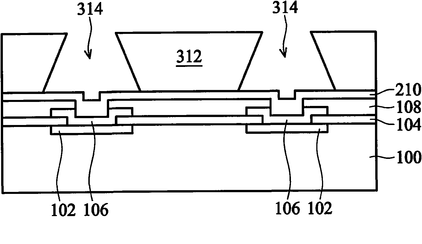
The invention provides a semiconductor device and a manufacturing method thereof. The semiconductor device comprises a first base material possessing a first inner connection structure and a second base material possessing a second inner connection structure. The first inner connection structure is in connection with the second inner connection structure, and a first width of the first inner connection structure is different fro that of the second inner connection structure. The invention provides a lug structure used foe connecting one base material with another one. A conductive cylinder is formed on the first base material such that the conductive cylinder has a different width from the that of a contact surface of the second base material. In one embodiment, the conductive cylinder of the first base material is a trapezoid or taper side wall, and thereby providing a conductive cylinder, the top of which is wider the the bottom. The base materials can be integrated circuit chips, pinboards, printed circuit boards, high density interconnectors and etc. The invention can reduce the delamination caused by Junction stress.

Description

technical field [0001] The present invention relates to an integrated circuit, a semiconductor device and a manufacturing method thereof, in particular to a bump structure for a semiconductor chip. Background technique [0002] Since the invention of the integrated circuit, the semiconductor industry has experienced rapid growth due to the continuous improvement in the integration of various electronic components (eg, transistors, diodes, resistors, capacitors, etc.). Primarily, these improvements in density come from repeated reductions in the minimum device size, allowing more devices to be integrated per unit area. [0003] These improvements in density are still two-dimensional (2D) in nature, with the volume occupied by integrated circuits being substantially only on the surface of the semiconductor wafer. Although drastic improvements in lithography have made the fabrication of two-dimensional integrated circuits feasible, there are still physical limits to the densit...

Claims


Application Information

Patent Timeline
IPC IPC(8): H01L23/00H01L21/60H01L23/488H01L21/48
CPCH01L2924/01006H01L2224/13139H01L2924/01075H01L24/14H01L2224/13025H01L25/0655H01L2224/13016H01L2224/0557H01L2224/1403H01L2924/01047H01L2924/01079H01L24/13H01L2224/16145H01L2924/01013H01L2225/06517H01L2225/06513H01L2924/01078H01L24/03H01L2224/13155H01L2224/1354H01L2225/06541H01L2224/1181H01L2224/13144H01L2224/16225H01L23/49811H01L25/0657H01L23/3192H01L2224/13169H01L2224/03452H01L2924/01074H01L23/3114H01L2224/14181H01L24/81H01L2225/06568H01L2224/1162H01L24/11H01L2924/01082H01L2224/05666H01L2224/81193H01L2224/11849H01L2224/0401H01L2224/11903H01L2224/0381H01L2224/1145H01L2224/11462H01L2924/01073H01L2224/73204H01L2224/13116H01L2924/01033H01L2224/11464H01L25/50H01L2224/05572H01L2924/01019H01L2224/11452H01L2224/11622H01L24/16H01L2924/014H01L2225/06548H01L2224/13084H01L2224/05647H01L2224/13111H01L2924/0105H01L2224/16227H01L2224/05681H01L2924/01029H01L2224/0345H01L24/05H01L24/73H01L2224/03831H01L2924/0002H01L2924/15788H01L2224/05552H01L2924/00H01L2224/11472H01L2224/13017H01L2224/16235H01L2924/14H01L21/486H01L23/49827H01L23/49838H01L23/5384H01L24/09H01L24/17H01L2224/16146
Inventor 沈文维施应庆陈承先陈明发
Owner TAIWAN SEMICON MFG CO LTD
Learn More